=================================================================================
The electrical potential of any observing structure can always be simplified to an equivalent circuit diagram consisting of a capacitance C and a resistance R to ground. The capacitance and resistance can be variable but it is fairly accurate if we just consider them as constants in normal SEM and FIB operation conditions. The net current between the beam-irradiating spot and the ground is the total current (It) of the incident beam and the emitted secondary electrons (SEs). The electrical potential of the observing structure can be modified from the format presented by other authors [1] and be given by,
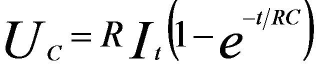 -------------------------- [3845a] -------------------------- [3845a]
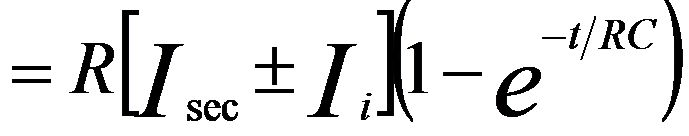 -------------------------- [3845b] -------------------------- [3845b]
“-” is applied when an electron beam is used as the incident beam, while “+” is applied when a positive ion beam is used as the incident beam.
Figure 3845 shows the schematic illustration of the current flows. The inset presents the electrical potential of the observing structure as a function of time. There are two potential thresholds: dark threshold (Ud) and bright threshold (Ub). If the resulted potential is higher than Ud the structure appears dark, while the structure appears bright if the potential is lower than Ub. The tscan is the scanning time of the incident beam.
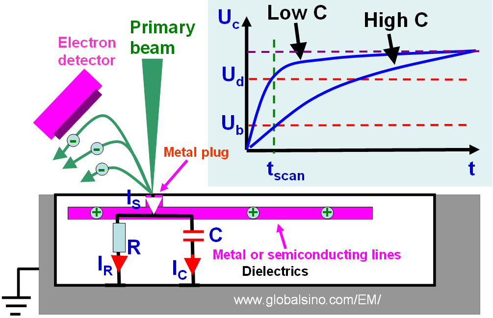
Figure 3845. Schematic illustration of the current flows of the equivalent circuit diagram. The inset shows
the potential of the observing structure as a function of time.
Some structures have very large capacitances. For instance, if a gate structure in MOS transistors or the structure which is connected to the gate is relatively large, they should be considered as a capacitor. Therefore, the duration which the gate or connected structure is exposed to the incident beam in FIB or SEM can be too short so that they are not significantly charged to affect their PVC.
[1] Ruediger Rosenkranz, Failure localization with active and passive voltage contrast in FIB and SEM, J Mater Sci: Mater Electron (2011) 22:1523–1535.
|