|
This book (Practical Electron Microscopy and Database) is a reference for TEM and SEM students, operators, engineers, technicians, managers, and researchers.
|
=================================================================================
Annular dark-field transmission electron microscopy (ADF-TEM) is widely used to evaluate the mass-thickness, atomic number and imaging of TEM samples. A simple ADF-aperture setup uses an annular objective aperture that acts as a central beam stop in the back focal plane of the objective lens [1 – 5] as shown in Figure 3892a. This aperture also blocks the outer electrons scattered at very high semiangles. Therefore, the central beam and all electrons scattered at very high semiangle are excluded from imaging. By optimizing the dimension of the inner and outer rings (~ 86 µm for the inner ring and ~200 µm for the outer ring in Figure 3892a), many applications can be obtained. The SEM (secondary electron microscopy) image in Figure 3892a (b) shows an annular aperture fabricated using focused-ion-beam (FIB) technique.
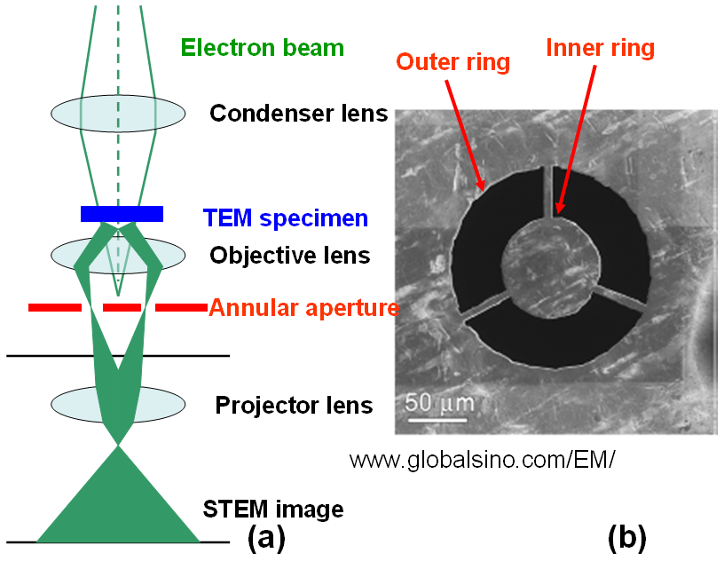
Figure 3892a. a) Schematic illustration of the column of a scanning transmission electron
microscope (STEM) system. b) An ADF aperture prepared using focused-ion-beam (FIB) technique.
The inner angles for HAADF detectors are at least three times the angle of electron-probe-forming aperture. In many cases of HAADF imaging, the annular detection angle was practically set to be 60 - 170 mrad due to the limitation of combinations between aperture sizes and camera lengths.
Figure 3892b shows the positions of the detectors which can be installed in a STEM system. Depending on the scattering angle of the transmitted electrons, various signals can be detected as a function of the position of the scanning probe: BF (bright-field)-STEM, DF (dark-field)-STEM or HAADF (high angle annular dark field)-STEM. The DF detectors are annularly shaped to maximize the collection efficiency and the range of the collected scattering angles can be adjusted through the magnification of the intermediate lenses.
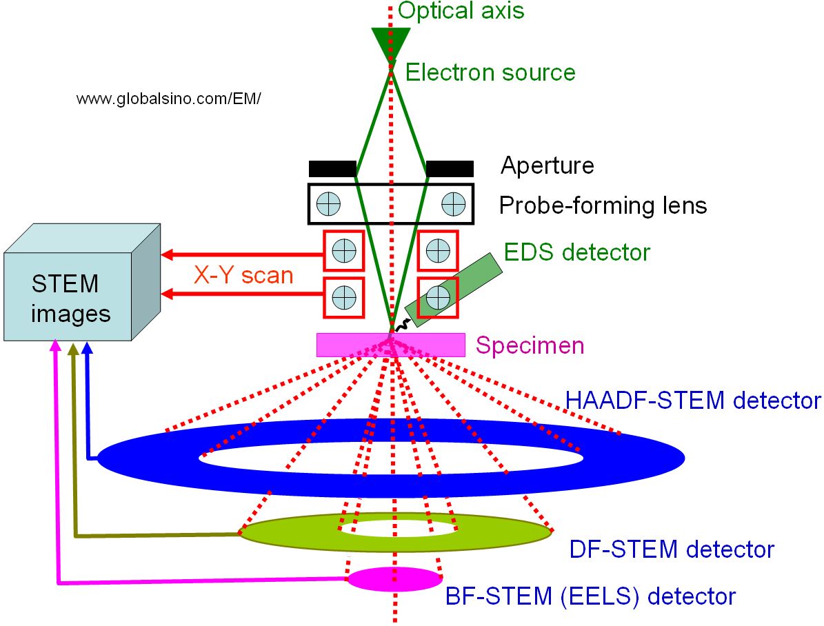
Figure 3892b. The positions of detectors in STEMs.
[1] K. Heinemann, H. Poppa, Phys. Rev. Lett. 1972, 20, 122.
[2] Z. L. Wang, A. T. Fisher, Ultramicroscopy 1993, 43, 183.
[3] Z. L. Wang, Ultramicroscopy 1994, 53, 73.
[4] S. Bals, B. Kabius, M. Haider, V. Radmilovic, C. Kisielowski, Solid
State Commun. 2004, 130, 675.
[5] S. Bals, R. Kilaas, C. Kisielowski, Ultramicroscopy 2005, 104, 281.
|