=================================================================================
The electrons generated by photons during the exposure time are collected in the wells in the sensors of CCD camera. The maximum number of electrons that a pixel can hold is determined by the full-well capacity and plays a dominant role in characterizing the CCD’s dynamic range. If the number of generated charges exceeds full-well capacity of a pixel during the exposure time, the extra charges will flow to the neighbor cells, meaning if these wells are saturated the extra charges will flow to the adjacent pixels. This process is called smearing or blooming, which induces fully saturated streaks on the image, destroying pixel information.
The parasitic intensity streaks correspond to the most intense peaks, and some parasitic oblique streaks originate mainly from the direct beam, for instance, as shown in Figure 3964a. These streaks are usually induced from detector memory effects and blooming during the acquisition of the pattern and from the type of shutter used for data acquisition [2]. This type of artifacts especially exist when the exposure time is very short and the signal intensity in some part of the diffraction pattern is very low.
![Parasitic artifacts in electron diffraction patterns: (a) Si [112], and (b) SrTiO3 [001]](image2/3087.JPG)
Figure 3964a. Parasitic artifacts in electron diffraction (ED) patterns: (a) Si [112], and (b) SrTiO3 [001]. [3] |
However, such streaks can be removed by proper programming, for instance, as shown in Figure 3964b.
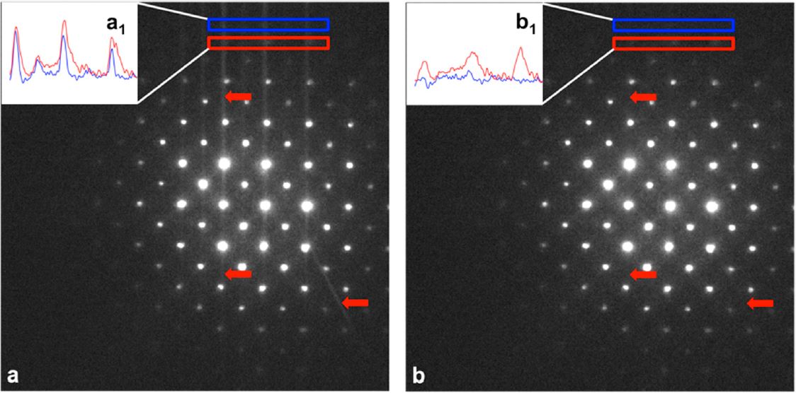
Figure 3964b. (a) Recorded ED pattern of SrTiO3 with some parasitic streaks pointed by red arrows, and (b) the pattern of SrTiO3 after a streak-removal procedure. [3] |
Figure 3964c also shows streaking artifacts presented in an TEM ED pattern recorded by a CCD camera.
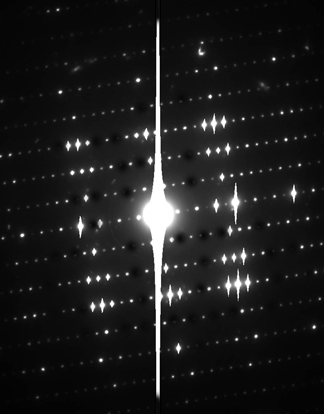
Figure 3964c. Streaking artifacts presented in an TEM electron diffraction pattern recorded by a CCD camera.
Note that the parasitic streaks sometimes can be reduced by changing the acquisition time.
[1] Senninger, D. Analysis of Electron Diffraction Patterns from Carbon Nanotubes with Image Processing
to Determine Structural Parameters. Ph.D. Thesis, University of Regensburg, Regensburg, Bavaria,
December 2011.
[2] Mollon, B.; Pan, M.; Jia, Y.; Mooney, P.; Sha, T. Development of a fast CCD camera for electron diffraction
imaging in conventional TEM. Microsc. Microanal. 2009, 15, 166.
[3] Francesco Scattarella, Liberato De Caro, Dritan Siliqi and Elvio Carlino, Effective Pattern Intensity Artifacts Treatment for Electron Diffractive Imaging, Crystals, 7, 186 (2017).
|