|
This book (Practical Electron Microscopy and Database) is a reference for TEM and SEM students, operators, engineers, technicians, managers, and researchers. You can click How to Cite This Book to cite this book. Please let Dr. Liao know once you have cited this book so that the brief information of your publication can appear on the “Times Cited” page. This appearance can also help advertise your publication.
|
=================================================================================
Changing the fringe spacing in electron holography can be categorized by two ways:
i) Enlarge the deflection angle in the electron biprism. However, the deflection angle is controlled by the applied voltage to the filament electrode, and the applied voltage is limited by the electric discharge, e.g. ≤ 300 V for some systems.
ii) Adjust the optical system. In this way, the fringe spacing is changed by turning off the current of the objective lens [1,2] or by controlling the distance between the electron biprism and the crossover position in an interferometer [3]. This is more promising way.
The fringe spacing in off-axis electron holography can be given by the intensity (I) in a format of cosinoidal interference pattern,
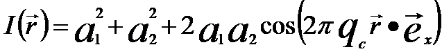 -------- [4202d] -------- [4202d]
where,
qc - Spatial frequency
(=kβ)
β -- The angle of the
superposition
Here, the cosinoidal term produces the fringes.
[1] Hasegawa S, Matsuda T, Endo J, Osakabe N, Igarashi M, Kobayashi
T, Naito M, and Tonomura A (1991) Magnetic-flux quanta in superconducting
thin films observed by electron holography and digital
phase analysis. Phys. Rev. B 43: 7631–7650.
[2] Bonevich J E, Harada K, Matsuda T, Kasai H, Yoshida T, Pozzi G,
and Tonomura A (1993) Electron holography observation of vortex
lattices in a superconductor. Phys. Rev. Lett. 70: 2952–2955.
[3] Wang Y Y, Kawasaki M, Bruley J, Gribelyuk M, Domenicucci A, and
Gaudiello J (2004) Off-axis electron holography with a dual-lens
imaging system and its usefulness in 2-D potential mapping of semiconductor
devices. Ultramicroscopy 101: 63–72.
|