=================================================================================
It was proposed [1] that the EELS ionization cross sections are within 5% for most K-edges and 15% for most L-edges, and the accuracy for other edges is significantly uncertain.
In some cases, the damage cross section (σd) is larger than the K-shel EELS ionization cross (σK) section, resulting in that the radiation damage prevents the detection of a single atom by K-shel EELS. If σd < σK, single atom detection is possible in principle.
Figure 4403 shows the comparison of the extracted EELS spectra of the N K-edge at 401 eV from a same region with the electron beam current of 150 pA and 850 pA, respectively, and from a crystalline TiN standard sample. Table 4403 shows the comparison of π* pre-peaks of the three cases in Figure 4403. This split is caused by the excitation of an N 1s electron in unoccupied t2g and eg orbitals formed by the hybridization of N 2p and Ti 3d electrons. [2] The high electron beam flux of 850 pA used for the data acquisition changed the chemistry and morphology in the analyzed region.
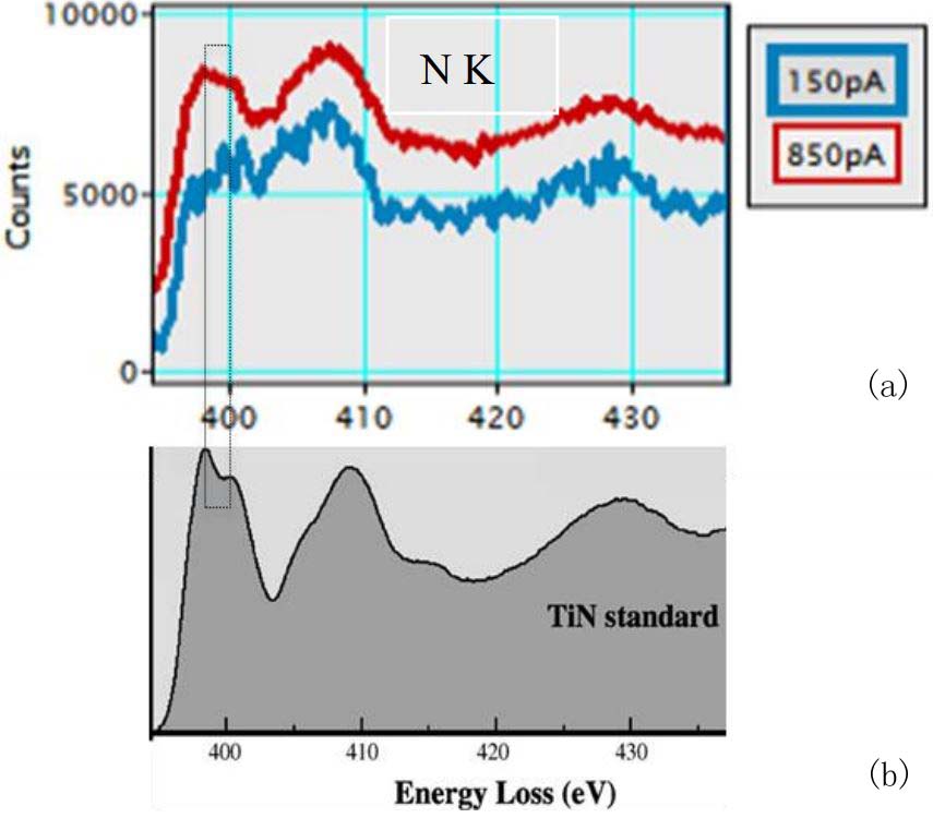
| Figure 4403. Extracted EELS spectra of TiN: (a) With an electron beam current of 150 pA, (b) With an electron beam current of 850 pA and (c) from a crystalline TiN standard sample. [2] |
Table 4403. π* pre-peak of the three cases in Figure 4403.
| |
π* pre-peak |
| With an electron beam current of 150 pA |
Appears to be weaker and no split |
| With an electron beam current of 850 pA |
Appears to be much stronger and more defined and is split by 2 eV |
| From a crystalline TiN standard sample |
[1] Egerton, R. F. (1993) Oscillator-strength parameterization of inner-shell cross sections.
Ultramicroscopy 50, 13–28.
[2] P. Longo, H. Zhang and R.D. Twesten, Simultaneous DualEELS and EDS Analysis Across the Ohmic Contact Region in FinFET Electronic Devices – Exploring the Effects of Electron Beam Damage, Microsc. Microanal. 22 (Suppl 3), 2016.
|