=================================================================================
Material characterizations usually attempt to link the specific aspects of the materials microstructure (e.g., crystalline
phase, particle shape and size, etc.) to its physical and chemical properties (e.g., electrical conductivity, selectivity, reactivity, etc.). Because the earliest characterizations were only conducted using optical microscopy, minimal structural information was obtained due to the limitation of its spatial resolution. However, by the mid-1920s de Broglie hypothesized that high-speed electrons exist as waves and that their wavelengths are shorter than visible light. Because the early TEMs were designed after the basic concept of a transmission light microscope with Köhler illumination, both systems have an illumination source, a series of lenses and apertures placed within their columns, a specimen stage, a viewing port, and an image recording system.
After both SEM and TEM were invented, TEM quickly became widely used to image replicas of surfaces at spatial resolution far better than was possible with the first SEM and thus further attempt to develop SEM was considered as a waste of time. Immediately after SEM became available commercially in 1965, it had widely been used to examine coatings, as seen in American Chemical Society Symposia on SEM of coatings in 1968 [1] and again in 1972 [2]. Later the higher resolution available from SEMs has mostly replaced TEM of surface replicas, however today TEM is growing faster than SEM because of the needs of ultra-high spatial resolution at nano-scale.
Table 4539.
Milestone of EM development.
DATE |
NAME |
MILESTONE |
1924 |
de Broglie |
High-speed electrons exist as waves |
Mid-1930s |
Knoll |
Designed a microscope in which its electron probe could be simultaneously
scanned over a specimen surface and synchronized with a cathode ray tube
(CRT) to produce an image |
1965 |
|
Commercial SEM |
Mid-1980s |
|
Personal computers (PCs) were used
to control slow speed CCD cameras in EMs |
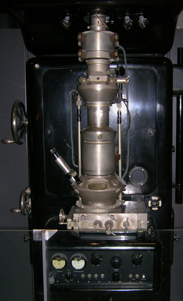
Figure 4539. Electron microscope built by Ernst Ruska 1933. |
[1] Prineen, L. H., Ed., "Scanning Electron Microscopy of Polymers
and Coatings," Applied Polymer Symposia, Vol. 16, 1968.
[2] Princen, L. H., Ed., "Scanning Electron Microscopy of Polymers
and Coatings," Applied Polymer Symposia, Vol. 23, 1974.
|