=================================================================================
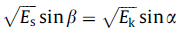
This refraction effect of secondary electrons (SEs) is given by [1],
 --------------------------------------------------- [4828a] --------------------------------------------------- [4828a]
Here, β -- the inner angle of incident electrons into the sample
α -- the
corresponding emission angle into the vacuum.
Es -- the SE kinetic
energy into the specimen
Ek -- the
corresponding kinetic energy into the vacuum
Based on Equation 4828a, Figure 4828 shows the schematic of angular SE transmission function, T(α), at the specimen/vacuum (S/V) interface in polar co-ordinates when the specimen is a metal, a semiconductor and an insulator.
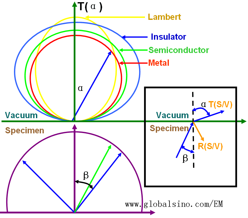
Figure 4828. Schematic of angular SE transmission function, T(α), at the specimen/vacuum (S/V) interface in polar co-ordinates when the specimen is a metal, a semiconductor and an insulator. The Lambert-type emission is also schematically shown for comparison. Adapted from [2]
The SE kinetic
energy into the specimen, Es, is given by
Es = Ek+ EF + Φ (for a metal) -----------------------------------------------[4828b]
Es = Ek+ χ (for a semiconductor or an insulator) ----------------------------[4828c]
Here, EF -- Fermi energy
Φ - - Work function
χ -- Electron affinity
The sum EF (Fermi energy) and Φ (Work function) for metals is often of ~10 eV.
Electron affinity, χ, for insulators is generally less than 3 eV.
[1] Henke, B.L., Liesegang, J. & Smith, S.D. (1979) Soft X-ray induced secondary
electron emission from semiconductors and insulators. Phys. Rev. B,
19, 3004–3021.
[2] J. Cazaux, (2005) Recent developments and new strategies in scanning electron microscopy, Journal of Microscopy, 217, 16–35.
|