=================================================================================
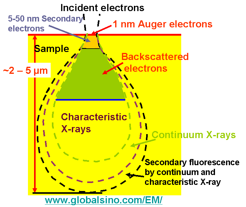 |
| Figure 4967. The interaction volumes for generations of secondary electrons, Auger electrons, backscattered electrons, characteristic X-rays, continuum X-rays, and secondary fluorescence (X-rays). |
The volume inside the specimen in which interactions occur while being struck with accelerating electrons. This volume depends on several factors such as atomic number of the materials of the specimen, accelerating voltage of the electron beam, and angle of the incident electron beam, because the materials with higher atomic number absorb or stop more electrons (having a smaller interaction volume), higher voltages penetrate farther into the sample and generate larger interaction volumes, and the greater the angle (further from normal) the smaller the volume. For comparison, Figure 4967 shows the interaction volumes for generations of secondary electrons, Auger electrons, backscattered electrons, characteristic X-rays, continuum X-rays, and secondary fluorescence (X-rays).
For silicon (Si), the interaction volume dimensions can vary from ~10 nm for 0.5 keV to several microns for 30 keV.
|