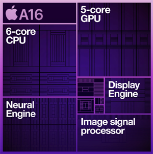
| The Apple A16 Bionic, shown in Figure 0152a, is a flagship processor used in the iPhone 15 and iPhone 15 Plus models. The Apple A16 Bionic processor contains nearly 16 billion transistors and is manufactured with 4-nanometer technology and features a six-core architecture.
The Apple A16 Bionic processor components are manufactured using TSMC’s 4 - 5 nm process technology. TSMC (Taiwan Semiconductor Manufacturing Company) produces the entire System on Chip (SoC) including the CPU, GPU, Neural Engine, display engine, and additional integrated features, as Apple relies on TSMC for its advanced process nodes for the A-series chips.
Apple itself is the designer for all components of the A16 Bionic processor, as it takes an integrated approach to designing the entire System on Chip (SoC) to optimize performance and efficiency across its devices. The processor includes two high-performance cores for intensive tasks like gaming and four energy-efficient cores for lighter tasks such as reading and video playback. The A16 Bionic processor primarily uses 6-transistor (6T) SRAM cells for its cache memory. This type of SRAM design is the industry standard for on-chip caches (e.g., L1, L2, and system-level caches) due to its balance of density, speed, and power efficiency.
The Apple A16 Bionic processor includes the following components:
- CPU cores. A 6-core setup with two high-performance cores (codenamed Everest) up to 3.46 GHz, and four power-efficiency cores (codenamed Sawtooth) up to 2.02 GHz. Apple designs the CPU cores (performance and efficiency cores) with custom architectures tailored to maximize performance per watt specifically for iOS devices. Both the performance and efficiency cores utilize SRAM for cache memory. The A16 Bionic has L2 caches for each core type (4 MB for efficiency cores and 16 MB for performance cores) and a System Level Cache (SLC) of 24 MB. These caches use SRAM to store frequently accessed data close to the processing cores, improving speed and reducing power consumption. Both the performance and efficiency cores in the A16 are expected to use 6T SRAM for their L2 caches and the SLC. The 6T configuration is compact and efficient, which is ideal for high-speed caching in the processor cores.
- Neural Engine: 16 cores with an increased performance of 17 TOPS (Tera Operations Per Second) for AI tasks. Apple develops this AI accelerator to handle machine learning and AI tasks natively within the chip, enhancing computational efficiency. Apple’s Neural Engine likely uses SRAM-based buffers and caches to facilitate high-speed data access during AI computations. SRAM is essential here because of its low latency, which supports the high-throughput demands of machine learning tasks.
- GPU: Integrated 5-core graphics engine. Apple designs the integrated GPU with custom configurations to ensure high graphics performance, particularly for applications like gaming and photo/video rendering. The GPU may use small amounts of embedded SRAM for caching display information or frame buffers, supporting tasks like anti-aliasing, adaptive refresh, and rendering. SRAM enables fast access to pixel and graphics data required for smooth performance.
- Display Engine: Supports adaptive refresh rates down to 1 Hz, enabling an always-on display and improved anti-aliasing for animations. Apple designs this to manage refresh rate adaptation and features like always-on display, ensuring compatibility with iOS animations and display technologies. The display engines may also use small amounts of embedded SRAM for caching display information or frame buffers, supporting tasks like anti-aliasing, adaptive refresh, and rendering. SRAM enables fast access to pixel and graphics data required for smooth performance.
- Memory: Utilizes LPDDR5 memory with a 50% improvement in memory bandwidth and includes 4 MB of L2 cache for efficiency cores, 16 MB of L2 cache for performance cores, and a 24 MB System Level Cache (SLC).
- Secure Enclave and Other Custom Features: ARMv8 instruction set, Machine Learning Controller, Secure Enclave, and Advanced Image Signal Processor (ISP). Custom features like the Secure Enclave, Machine Learning Controller, and Advanced Image Signal Processor are also designed by Apple to enhance security, machine learning, and image handling across Apple devices. The Secure Enclave, Machine Learning Controller, and Image Signal Processor likely incorporate SRAM for dedicated caches. SRAM in these parts enhances data security, quick processing, and minimizes power consumption by holding sensitive or frequently accessed data near processing elements. For security and custom processing, the 6T SRAM design remains optimal due to its balance between area efficiency and quick access times, both important for secure operations and minimal latency.
Figure 0152a. (a) Apple A16 Bionic, and (b) Main components in A16 [1]. |
For Yield Enhancement Engineering (YEE) of Apple A16 chips, the procedure would involve several targeted steps to systematically address yield losses throughout the fabrication and packaging processes. Given the complexity and scale of producing A16 chips on the advanced 4nm process, yield enhancement would follow these core steps:
- Yield Data Collection and Analysis
- Initial Data Collection: Gather defect density, particle contamination, and fail bin data from fab, sort, and final test stages.
- Statistical Analysis: Use statistical process control (SPC) to track and analyze defect distribution patterns and identify trends or spikes.
- Failure Analysis (FA): Analyze defective units to determine failure root causes, potentially involving physical failure analysis (PFA) and electrical fault isolation (EFI).
- Defect Pareto Analysis: Build a defect pareto chart to prioritize the most frequent and impactful defect types (e.g., lithography misalignments, etch residues, contamination).
- Inline Process Monitoring and Control
- Critical Process Step Inspection: Perform targeted inspections using SEM, AFM, or defect inspection tools at key process steps (e.g., lithography, etch, deposition) to detect early-stage yield detractors.
- Statistical Monitoring: Continuously monitor process metrics (critical dimensions, layer thicknesses, etc.) against established tolerances to detect drift.
- Equipment Maintenance and Calibration: Ensure all equipment is precisely calibrated, especially at process bottlenecks, to prevent equipment-induced variability.
- Defect Reduction and Process Optimization
- Root Cause Analysis (RCA): Identify and address root causes of dominant defects (e.g., particle sources, mask misalignment, chemical impurities).
- Process Refinement: Optimize process recipes based on RCA findings. This could involve adjusting photoresist formulations, modifying etch profiles, or tightening deposition uniformity.
- Contamination Control: Enhance cleanroom protocols, introduce more stringent particle monitoring, and minimize handling or exposure to contaminants at critical stages.
- Electrical Yield Learning
- Parametric Testing: Perform parametric tests (leakage, resistance, capacitance) to capture deviations, especially on high-density, power-hungry components like CPU/GPU and Neural Engine cores.
- Burn-In and Stress Testing: Run burn-in testing to detect latent defects that might fail over time, often caused by poor materials or weak interconnects.
- Feedback Loop with Design: Share data with the design team to identify potential design optimizations or redundancies, such as voltage tolerance adjustments in high-activity areas.
- Test and Measurement Improvement
- Advanced Test Algorithms: Develop adaptive testing for defect-prone modules (e.g., using machine learning algorithms for pattern recognition).
- Wafer-Level Testing: Implement thorough wafer-level test screening before packaging to eliminate low-yield wafers and prevent packaging unnecessary chips.
- Bin Analysis and Yield Mapping: Use detailed bin analysis to map fail locations and identify recurring patterns at wafer, reticle, or die level.
- Continuous Feedback and Design for Yield (DfY) Improvements
- Collaborate with Design Teams: Work with design engineers to enhance robustness in areas like power management, thermal handling, and layout adjustments.
- Redundancy and Fault Tolerance: Integrate design redundancies (e.g., spare cores, defect-tolerant cache) to increase effective yield.
- Iterative Learning Cycles: Establish iterative learning with feedback from every production batch to refine and improve yield continuously.
- Final Yield Monitoring and Continuous Improvement
- Yield Reporting: Regularly document yield data, compare it against historical baselines, and set new targets.
- Root Cause Corrective Action (RCCA): For each batch, perform RCCA on critical defects, implementing both short-term and long-term fixes.
- Supplier and Material Quality Control: Monitor suppliers (e.g., materials, photomasks) for consistency, and enforce high standards for incoming materials to reduce material-induced defects.
- Risk Assessment and Mitigation
- Scenario Analysis: Conduct risk assessments for potential process or equipment changes, incorporating yield risks in cost-benefit analysis.
- Contingency Planning: Prepare contingency plans to handle yield losses due to unexpected challenges (e.g., yield fallout on key lithography steps or unexpected contamination events).
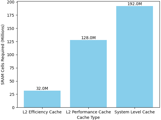
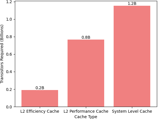
Estimating the exact number of SRAM cells in the Apple A16 Bionic is complex, as it depends on the detailed architecture of each cache and memory component (e.g., L2 caches, System Level Cache, and additional buffers for the Neural Engine, GPU, etc.). However, we can provide an approximate range based on typical cache sizes and the structure of 6-transistor (6T) SRAM cells:
- Cache Memory Sizes:
- L2 Cache: The A16 has 4 MB of L2 cache for the efficiency cores and 16 MB for the performance cores.
- System Level Cache (SLC): The SLC is 24 MB.
- SRAM Cell Calculation:
- Each bit in SRAM requires a 6-transistor (6T) cell.
- 1 MB of SRAM equals roughly 8 million bits, meaning it requires approximately 48 million transistors (since each bit has 6 transistors).
- 1 byte = 8 bits.
- Therefore, 1 megabyte (MB) = 1 million bytes = 8 million bits.
- Approximate Total SRAM Cells:
- L2 Caches: (4 MB + 16 MB) = 20 MB → 20 MB × 8 million cells/MB ≈ 160 million SRAM cells.
- System Level Cache: 24 MB → 24 MB × 8 million cells/MB ≈ 192 million SRAM cells.
Adding these, the A16 would have approximately 352 million SRAM cells for the primary cache structures alone. Other smaller caches in the GPU, Neural Engine, and additional components would add to this count, so the total SRAM cell count is likely higher than this estimate, possibly reaching around 400 million SRAM cells across the entire chip.
 |
 |
(a) |
(b) |
Figure 0152b. (a) Estimated SRAM cell counts for A16 cache sizes, and (b) Estimated transistor counts for A16 cache sizes. |
[1] restore.bg/.
|