| Figure 0173a illustrates the layout and equivalent circuit of a 6T SRAM cell embedded in a 0.25-μm generation microprocessor. [1] The left side of the figure shows the physical layout of the SRAM cell, and the right side shows the equivalent circuit schematic. This SRAM cell design is used in an application for high-frequency and low-voltage modes.

Figure 0173a. 6T SRAM cell layout embedded on a 0.25-μm generation microprocessor (left) and its equivalent circuit (right). Adapted from [1] |
The output of a read operation in SRAM is typically routed from either the bitline (BL) or bitline-bar (BL-bar), depending on the state of the cell's data. When reading, the selected cell are mirrored on both the bitline and bitline-bar, where one will represent the data (logic high or low) and the other its complement. The sense amplifier connected to these lines interprets the differential signal and amplifies it to drive the output pin, ensuring accurate data retrieval.
The 6T SRAM cell stores a single bit of data by holding it in a stable state within a cross-coupled inverter pair. Table 0173 shows the truth table for such a 6T SRAM cell.
Table 0173. Truth table for such a 6T SRAM cell presented in Figure 0173a.
| Operation |
Tr-NMOS Gates |
Drain of Tr-NMOS |
Drain of Tr-NMOS |
Node Q |
Node QB |
| Tr-NMOS |
WL (Word Line) |
Tr-NMOS |
BL (Bit Line) |
Tr-NMOS |
BLB (Bit Line Bar) |
| Hold |
Off |
Low |
|
— |
|
— |
Stable (either 0 or 1) |
Stable (either 0 or 1) |
| Read '1' |
|
High |
|
High |
|
Low |
High |
Low |
| Read '0' |
|
High |
|
Low |
|
High |
Low |
High |
| Write '1' |
|
High |
|
High |
|
Low |
High |
Low |
| Write '0' |
|
High |
|
Low |
|
High |
Low |
High |
In the 6T SRAM cell shown in Figure 0173a, during a read operation to detect a stored '1,' the cell operating conditions, as shown in Figure 0173b, are as follows:
- Assume:
- Word Line (WL) is low (=0).
- Q is low (=0), thus QB is high (=1).
- Activated Transistors:
- The two access transistors (Tr-NMOS) are activated by the Word Line (WL), which connects the storage nodes to the bit lines (Data Lines) for reading.
- The load PMOS transistor (Ld-PMOS) connected to the node storing "1" will be on (active) to pull the node to Vcc, thus representing a stable high state.
- Non-Activated Transistors:
- The driver NMOS transistor (Dr-NMOS) on the same side as the "1" state is off (inactive), as it does not need to pull the node to ground.
- On the opposite side (storing "0"), the Ld-PMOS is off, and the Dr-NMOS is on to pull that node to ground, maintaining the "0" state.
- Precharged Lines:
- Both bit lines (Data Lines) are precharged to a high voltage level (usually Vcc) before the word line is activated. This precharge allows the sense amplifier to detect a differential voltage change when the access transistors connect the storage nodes to the bit lines. The precharging process does not directly activate the transistors inside the SRAM cell (like the Tr-NMOS, Ld-PMOS, and Dr-NMOS transistors). Instead, it is typically managed by a precharge circuit outside the SRAM cell that pulls the bit lines to Vcc.
- During reading:
- BLB is precharged to VCC/2, while BL is discharged to ground as shown in Figure 0173c. During a read operation, the bit-lines are initially precharged to a common intermediate voltage before accessing any cell. This precharge process, however, can be relatively slow due to the limited drive strength of the minimized transistors within each cell, which are designed for high density rather than speed. Once the cell is accessed, a small differential voltage develops between BL and BLBar, reflecting the stored data. At this stage, the sense amplifier plays a critical role, not by accelerating the precharge itself, but by rapidly detecting and amplifying this small differential signal to drive it to a full logic level.
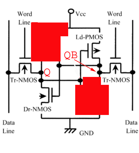
Figure 0173b. Read operation to detect a stored "1". The hidden transistors are not activated. For this case, data lines are precharged to Vcc. |
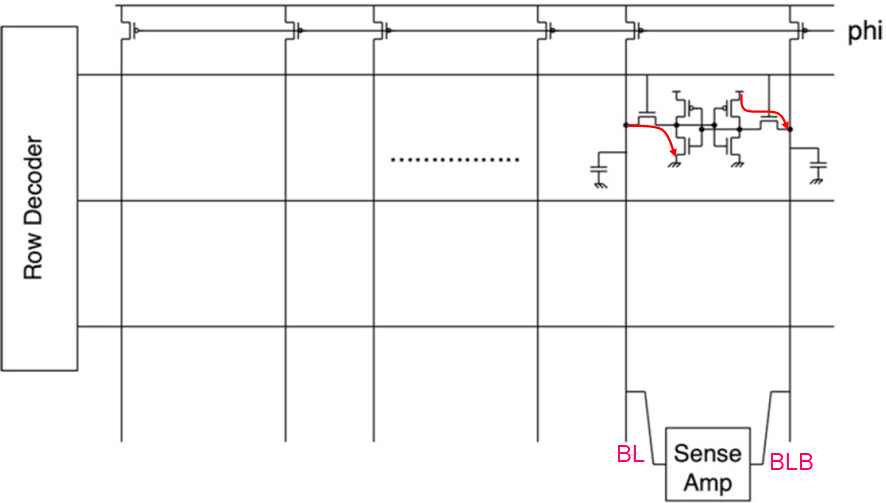
Figure 0173c. Equivalent circuit model for cell delay. Adapted from [2] |
In details, the operation steps during a read operation to detect a stored "1" are:
- Step 1 (see Figure 0173d):
- Word Line (WL) is low (=0).
- Q is low (=0), thus QB is high (=1).
- Data line is high (=1).
- Results: Tr-NMOSs are off.
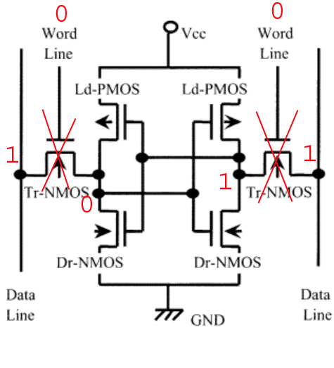
Figure 0173d. Initial state of the 6T SRAM cell. |
-
Step 2:
- Word Line (WL) is high (=1).
- Q is low (=0), thus QB is high (=1).
- Results: The voltage of the data line on the left goes down, and the voltage at Q goes up as shown in Figure 0173e; however, GND tries to pull Q to 0 so that Q will be back to 0. Figure 0173f shows the waveform during this operation step.

Figure 0173e. Reading "1". |

Figure 0173f. Waveform during the operation step of a read operation to detect a stored "1". |
The transistors that are activated and not activated during a read "0" operation are different from those in a read "1" operation in the 6T SRAM cell:
- During Read "1":
- Activated:
- Access transistors (Tr-NMOS) on both sides (because the Word Line is activated).
- Load PMOS (Ld-PMOS) on the side storing "1" (to pull the node to Vcc).
- Not Activated:
- Driver NMOS (Dr-NMOS) on the "1" side (as it doesn't need to pull the node to ground).
- Load PMOS (Ld-PMOS) on the "0" side (since the node is already grounded by Dr-NMOS on that side).
- During Read "0":
- Activated:
- Access transistors (Tr-NMOS) on both sides (because the Word Line is activated).
- Driver NMOS (Dr-NMOS) on the side storing "0" (to pull the node to ground).
- Load PMOS (Ld-PMOS) on the "1" side (to keep that node at Vcc).
- Not Activated:
- Driver NMOS (Dr-NMOS) on the "1" side (as it doesn't need to pull the node to ground).
- Load PMOS (Ld-PMOS) on the "0" side (since the node is already pulled to ground by Dr-NMOS on that side).
[1] Ikeda, S., Yoshida, Y., Ishibashi, K., & Mitsui, Y., Failure Analysis of 6T SRAM on Low-Voltage and High-Frequency Operation. IEEE Transactions on Electron Devices, 50(5), 1270–1276, 2003.
[2] Karim Abbas, Handbook of Digital CMOS Technology, Circuits, and Systems, 2020.
|
