iPHEMOS HAMAMATSU Failure Analysis System is an inverted emission microscope, which is a backside analysis system designed to identify failure locations by
detecting the light photoemission and heat (thermal signal) emitted from the defects of failures in semiconductor devices.
The signal detection from backside facilitates the use of probing and probe card to the wafer surface.
The platform, allowing to mount multiple detectors and lasers, enables the selection of the optimum detector for
performing various analysis methods such as:
i) light emission,
ii) heat generation analysis,
iii) IR-OBIRCH analysis,
iv) permitting dynamic analysis perform efficiently by tester (LSI tester, see Figure 4927b) connection with multi-pin needle
contact by a probe card. By connecting directly to the LSI tester, signal delay due
to the connection cable length can be reduced, and the
analysis of high-speed driving samples becomes possible.
the iPHEMOS systems have:
i) Two ultra-high sensitivity cameras which cover different detection wavelength ranges needed for emission analysis (near-infrared range) and thermal analysis (mid-infrared range).
ii) High sensitivity macro lens and up to 10 lenses.
iii) With options:
iii.a) Includes laser scan system
iii.b) Emission analysis with high-sensitivity near-infrared camera
iii.c) Thermal analysis with high-sensitivity mid-infrared camera
iii.d) IR-OBIRCH analysis
iii.e) Dynamic analysis by laser irradiation
iii.f) EO probing analysis
iii.g) High-resolution and high-sensitivity analysis using NanoLens
iii.h) Connects to CAD Navigation
iii.i) Connects to LSI tester.
iv) Display functions:
iv.a) Annotations.
Comments, arrows, and other indicators can be displayed on an
image at any location desired.
iv.b)
Scale display.
The scale width can be displayed on the image using segments.
iv.c)
Grid display.
Vertical and horizontal grid lines can be displayed on the image.
iv.d)
Thumbnail display.
Images can be stored and recalled as thumbnails, and image
information such as stage coordinates can be displayed.
iv.e)
Split screen display.
Pattern images, emission images, superimposed images, and
reference images can be displayed in a 4-window screen at once.
iv.f) Flexible scan: Normal scan (1024 × 1024, 512 × 512), Zoom, Slit Scan, Area Scan, Line Scan, Point Scan, Scan direction is changeable
(0°, 45°, 90°, 180°, 270°).

Figure 4927a. iPHEMOS HAMAMATSU Failure Analysis System. [1]

Figure 4927b. iPHEMOS-DD with a LSI tester. [1]
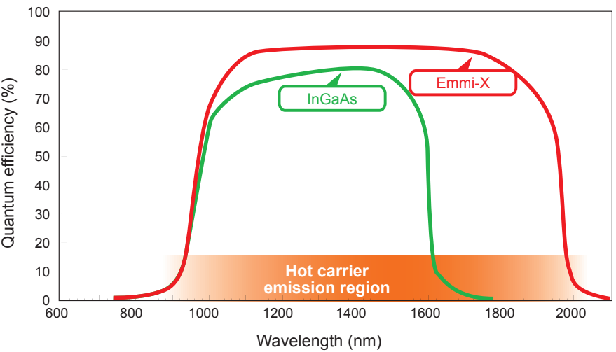
Figure 4927c. Comparative chart of wavelength sensitivity ranges. [1]
Due to the ultra-miniaturization and higher integration
of semiconductor devices and their low-voltage operation, the
infrared light from heat emitted at failure locations has become
increasingly weak and difficult to detect. However, the detection of high sensitivity in the mid-infrared range
with InSbHS and ThermoDynamicV2 cameras
can pinpoint those weak thermal emissions. Thermal emission can be used:
i) Identifying thermal emission locations,
ii) Short-circuits in metallic layers and wiring,
iii) Abnormal resistance at contact holes,
iv) Microplasma leakage in oxide layer,
v) Oxide layer breakdown,
vi) LCD/organic EL leakage, ,
vii) lock-in analysis, (e.g. see Figure 4927e)
viii)
thermal conductive properties of the device layer materials.

Figure 4927d. Thermal lock-in measurement (also called Lock-in thermography (LIT)). [1]
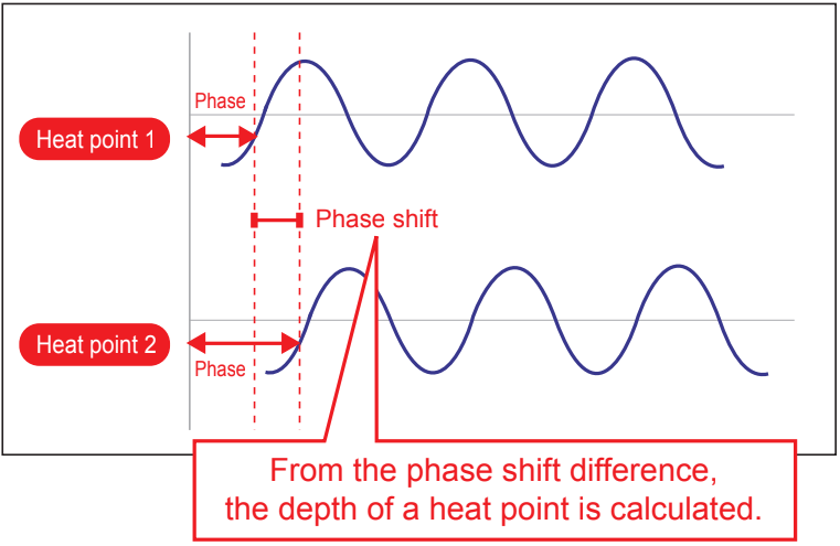
Figure 4927e. Calculation of depth of a heat point. [1]
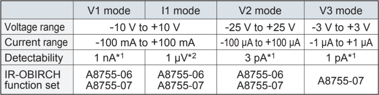
| Table 4927. Selectable V1 mode, I1 mode, V2 mode, and V3 mode in IR-OBIRCH analysis with iPHEMOS series. [1] |
[1] Overview of function of iPHEMOS series.
|