Chapter/Index: Introduction | A | B | C | D | E | F | G | H | I | J | K | L | M | N | O | P | Q | R | S | T | U | V | W | X | Y | Z | Appendix
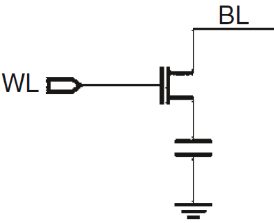
| In all memories, cell data is always transferred through the bit line in y-axis (also called digitline), and the word line in x-axis is used to select the cell. [1] Figure 4993a shows a so-called 1T1C modern DRAM memory bit, which is formed with one transistor and one capacitor. The transistor operates as a switch between the capacitor and the digit line. The capacitor’s common node is biased at Vcc/2. Storing a logic “1” in the cell requires the capacitor to have a voltage of +Vcc/2 across it. Storing a logic “0” in the cell requires the capacitor to have a voltage of –Vcc/2 across it. Therefore, in both cases, the stored charge across the capacitor is the same in an absolute value, but the charges are opposite.
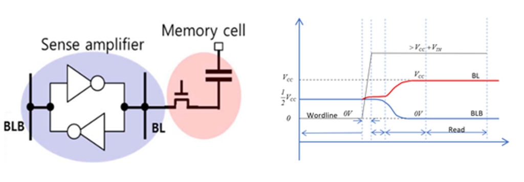
The read process of all memory devices is common. After settling the predefined voltage to the bit line, the bit line is electrically connected with the memory cell. Then, the stored bit information of the cell will modulate the bit line voltage or current. The modulated analog value (voltage or current) of a bit line is then converted to the digital value (namely, GND or VDD) by the sense amplifier (SA) circuit. Since the DRAM cell is a capacitor, the charge sharing process can modulate the bit line voltage as shown in Figure 4993b. [1]
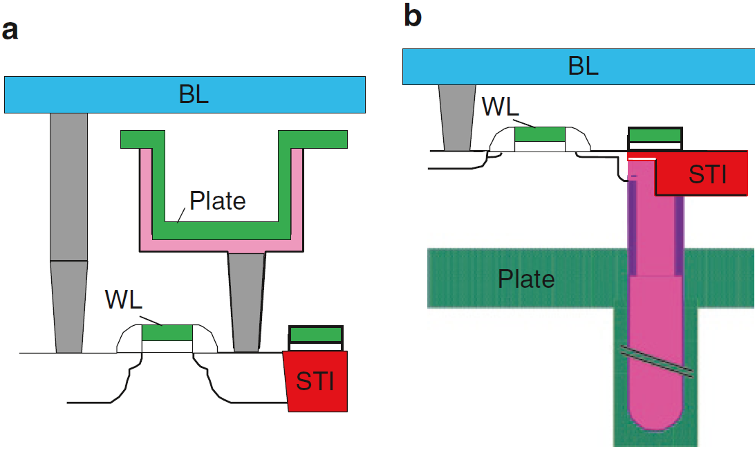
Figure 4993b. DRAM and its equivalent circuit models. [1] Figure 4993c shows the cross-section view for (a) stacked DRMA cell and (b) trench DRAM cell. Historically, a stacked cell approach [2] was commonly used for commodity DRAMs. However, in this structure, the capacitor over the device is built after the device has been built, which makes it difficult to keep the logic transistor performance. On the other hand,, it is difficult to planarize the surface of the silicon due to the stacked capacitor. Furthermore, if the wiring rule is changed, most logic library elements need to be redeveloped, which can be expensive. This may cause performance degradation due to wiring capacitance and resistance delays. The trench capacitor in Figure 4993c (b) can be fabricated by digging the hole in the silicon before the device has been built. This method will allow for a fully compatible process to logic technology and will not degrade transistor performance, giving an ideal technology solution for embedded DRAM integration in a logic chip. [3]
Figure 4993d shows a cross-sectional view of the 256 Mbit buried strap DRAM cell.
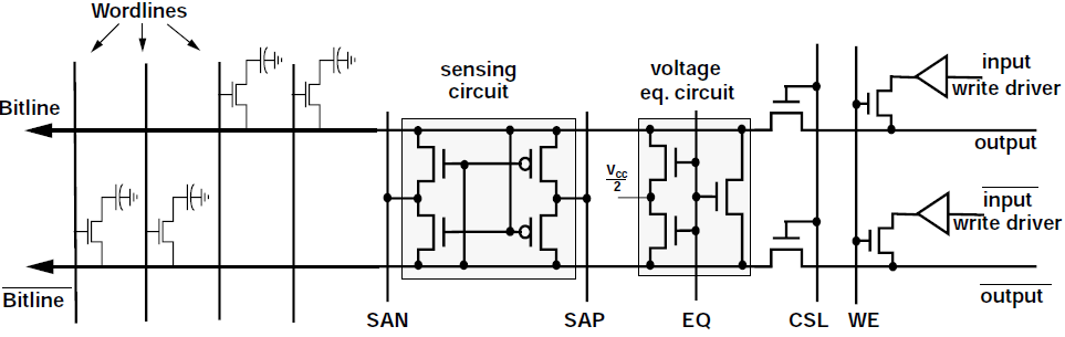
Figure 4993e shows two examples of sense amplifiers. The selection criterion of sense amplifiers is determined by the circuit area and operating speed.
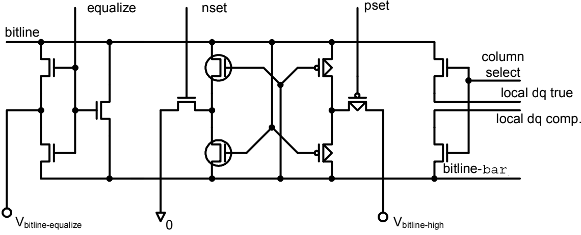
Latch in a SA will be working as the logic circuit not the analog circuit, so that its operation is very robust to the process variations. Since many numbers of a SA will bring the large leakage current, then it is necessary to control some device parameters related to the threshold voltage such as doping density, channel length and width, etc. Figure 4993f shows a diagram of a basic sense amplifier. More complex sense amplifiers in modern DRAM devices contain the basic elements, as well as additional circuit elements for array isolation, careful balance of the sense amplifier structure, and faster sensing capability. In Figure 4993f, the equalization (EQ) signal line controls the voltage equalization circuit. The functionality of this circuit is to ensure that the voltages on the bitline pairs are as closely matched as possible. Since the differential sense amplifier is designed to amplify the voltage differential between the bitline pairs, thus any voltage imbalance that exists on the bitline pairs prior to the activation of the access transistors would degrade the effectiveness of the sense amplifier. [6]
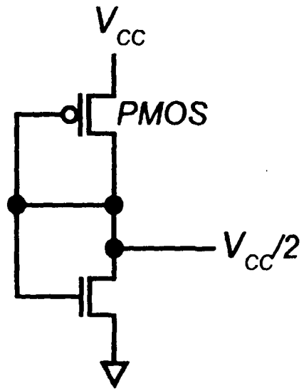
Figure 4993f. Diagram of a basic sense amplifier. [6] Memory capacitor in DRAM is biased to VCC/2, and the digitlines are always equilibrated and biased to VCC/2 between array accesses. Therefore, DVC2 voltage refers to a voltage level at half the level of the DC supply voltage. In most DRAM designs, the cellplate and digitline bias voltages are derived from the same generator circuit. Figure 4993g shows a simple circuit, for generating VCC/2 (DVC2) voltage, which is composed of a standard CMOS inverter with the input and output terminals shorted together. With correct transistor sizing, the output voltage of this circuit can be accurately set to VCC/2 V.
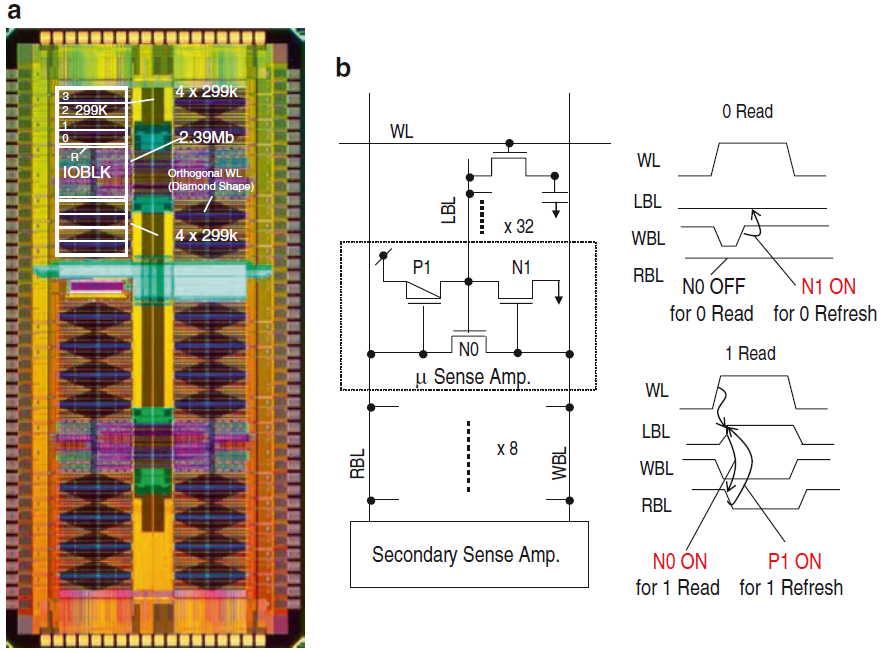
2.39 Mb embedded DRAM (eDRAM) macros [3] shown in Figure 4993h are organized by upper and lower memory units, each consisting of four 299 Kb sub-arrays (0 through 3) and a 16 row redundancy array (R). They are supported by the Input and Output circuitry (IOBLK) located between two memory units. When the macro decoder receives a valid macro-select-signal and a valid read or write command, then the decoder evaluates the address, activating either the top or bottom memory units. The activation of the memory unit enables one of the four arrays, and sends 1 of 256 valid addresses. The 299 Kb sub-array includes ECC bits for IBM servers. An evolutionary approach in this eDRAM locates the segmented WL drivers in the sense amplifier area, which couples to the horizontally arranged WLs through the vertically arranged wires.
The term sense amplifier refers to a collection of circuit elements that pitch up to the digitlines of a DRAM array. This collection most generally includes isolation transistors, devices for digitlines equilibration and bias, one or more Nsense-amplifiers, one or more Psense-amplifiers, and devices connecting selected digitlines to I/O signal lines. All of the circuits along with the worldline driver circuits are called pitch cells. [5] Each memory with 2k cells is composed of 64 wordlines and 32 bitlines for 2,048 memory elements/address locations per aπay. When a voltage is applied voltage on the word line (WL) and the transistor is turned on, the charges are stored in the capacitor through the bit line. At this time, when a high voltage(Vdd) is applied to the bit line (BL), DATA 1 is stored in the capacitor, and when a low voltage (Vss, 0 V) is applied, DATA 0 is stored. When reading stored data, the bit line(BL) and bit line bar(BLB) are compared: The BLB becomes a standard point because it is not connected to the cell. Because the signal difference between BL and the BLB is very small, it is amplified through the sense amplifier circuit to read data as shown in Figure 4993i.
As shown in Figures 4993j and 4993k, a typical bitline sense-amplifier stripe has 11 transistors per bitline pair, a typical local wordline driver stripe has 3 transistors per local wordline. The share of bitline sense-amplifier area to total die area in a typical DRAM die is between 8% and 15%, the share of local wordline driver area is between 5% and 10%.
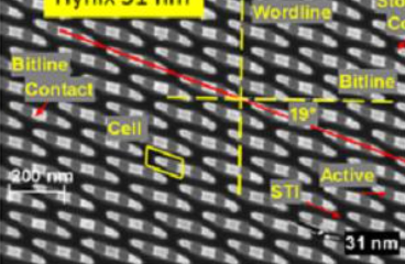
In the process integration of D1z 12 Gb LPDDR5 DRAM devices, Samsung adopted EUV lithography technology limited to only one mask, a Storage Node Landing Pad (SNLP on call array)/Bit Line Pad (BLP on S/A) which measures around 40 nm critical dimension (CD or pitch) and 13.5 nm BLP line width on S/A (sense amplifier circuitry) area. [3] Figure 4993l shows a comparison of S/A BLP patterns with ArF-i based lithography and with EUV lithography (EUVL) from Samsung. By using EUV lithography, BLP line edge roughness (LER) on S/A area is improved and bridge/short defects might be reduced.
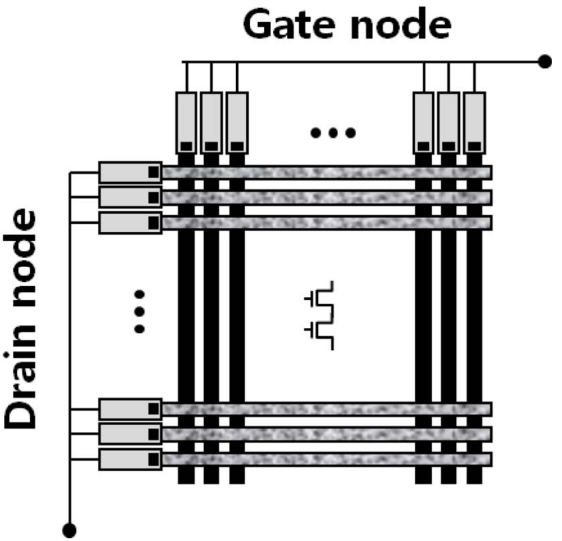
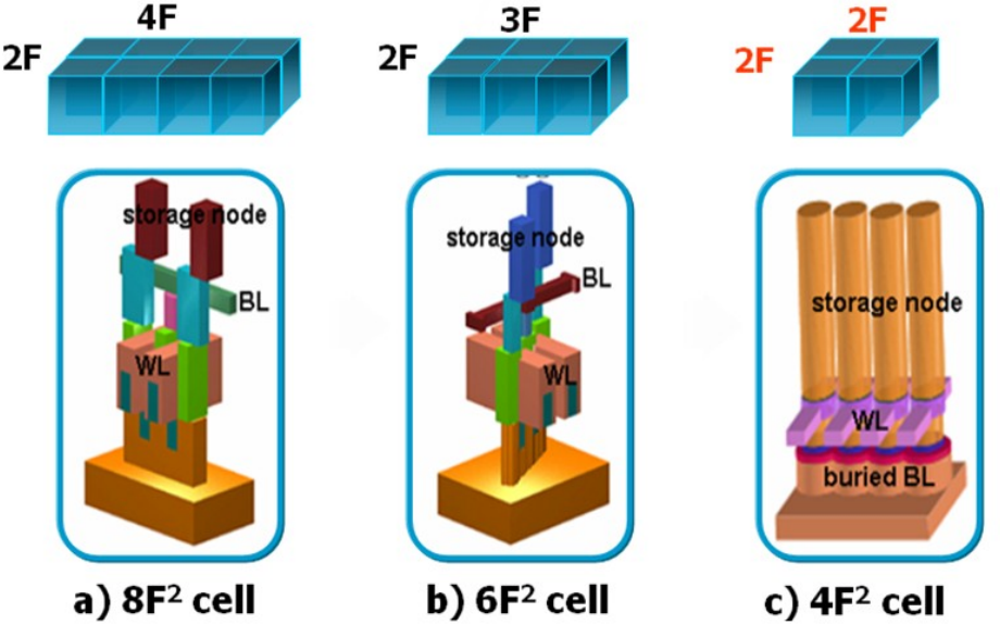
Figure 4993m. Gate (WL) and drain (DL) nodes in DRAM. [12] The cell architecture shown in Figure 4993n has been evolved from 8F2 cell to 6F2 cell since the cell size could be reduced up to 75% at the same design rule (F). [13]
Figure 4993o. DRAM cell transistor in BCAT structure. Adapted from [14] Figure 4993p shows DRAM 8F2 cell structure:
Figure 4993p. DRAM 8F2 cell structure. [14]
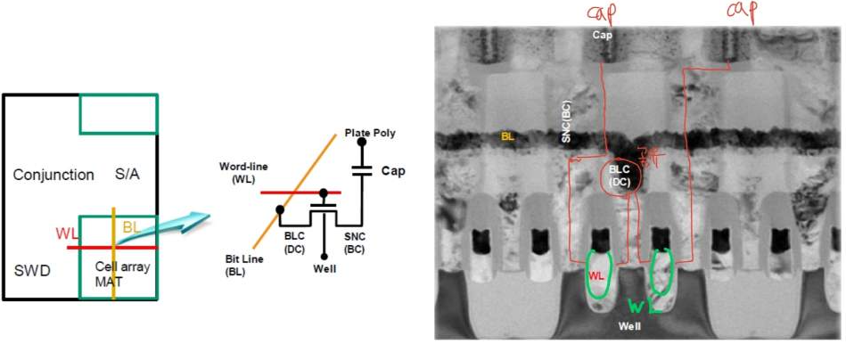
Figure 4993q. Structure of DRAM and peripheral circuitry. [14]
Figure 4993t shows Samsung DRAMs. In the 48-nm version, since the hard mask, which is normally on top of the BL, is not used or has been removed, the height of the capacitor contact plug and its series resistance are reduced.
Figure 4993u shows bitline and wordlines in Winbond 65-nm 1 Gb SDRAM. The bitline has a stack of W and poly-Si layers.
[1] Krzysztof (Kris) Iniewski, CMOS Processors and Memories, (2010).
|