Incomplete Charge Collection in EDS Measurements - Practical Electron Microscopy and Database - - An Online Book - |
||||||||||||||||||||
| Microanalysis | EM Book http://www.globalsino.com/EM/ | ||||||||||||||||||||
| ================================================================================= | ||||||||||||||||||||
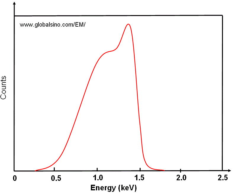
Silicon (Si) has a large mass absorption coefficient, especially for low energy photons, resulting in shallow depth of absorption in the EDS detectors, and thus a significant portion of the absorption happens in the dead layer. For instance, if a photon is absorbed in the partially active Si just underneath the surface electrode or the sides of the X-ray detector, the collection of charge carriers is then imperfect and thus the loss of some electron-hole pairs due to trapping and recombination at the defects results in an underestimate of the photon energy. These photons induce a distortion of the low-energy side of the peak from the ideal Gaussian shape, known as "incomplete charge collection". This incomplete charge collection leads to such characteristic asymmetry of peak: high end of the peak is sharp while low end of the peak tails. Such effects are most severe for low energy photons (e.g. energies less than 3 keV, especially at < 1 keV). Note that some simulators, e.g. Monte Carlo method [1], can include the effect of incomplete charge collection within the Si dead layer. The measured X-ray line shape P(E) as a function of the analyzed photon energy E, can be given by the Hyperment function, For instance, Figure 1756a shows an Al Kα (1.486 keV) EDS profile obtained with an old HpGe detector. This severe distortion of the peak shape and the large shift of the peak position due to extremely incomplete charge collection make the measurements at energies below ~2 keV (especially just above the energy of Ge L absorption edges from 1.2 to 1.4 keV) impossible.
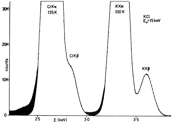
The EDS spectrum of KCl in Figure 1756b shows a peak overlap and a typical spectrum distortion induced by the incomplete charge collection. The chlorine Kα and Kβ peaks are not resolved, while the potassium Kα and Kβ are almost resolved. The solid line is a Gaussian fit to the data points. The shaded areas are two non-Gaussian low energy tails that are distortions induced by incomplete charge collection.
Table 1756. Summary of reported incomplete charge collections of X-rays in EDS measurements.
[1] Raynald Gauvin and Eric Lifshin, On the simulation of true EDS X-ray spectra, 430, Proceedings: Microscopy and Microanalysis 2002, edited by Edgar Völkl.
|
||||||||||||||||||||
| ================================================================================= | ||||||||||||||||||||
|
|
||||||||||||||||||||