Chapter/Index: Introduction | A | B | C | D | E | F | G | H | I | J | K | L | M | N | O | P | Q | R | S | T | U | V | W | X | Y | Z | Appendix
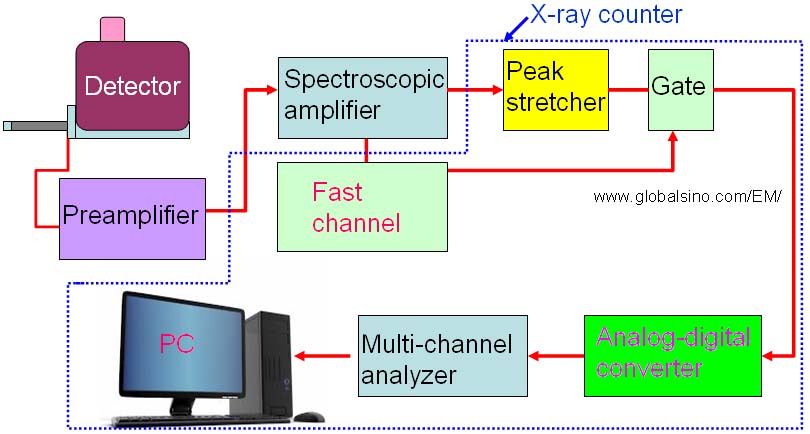
| The energy dispersive system for photon detection has normally a semiconducting detector with high impedance materials that is radiation-sensitive. Both the detector and field-effect transistor (FET) of the first stage of preamplifier are cooled to get an optimum of energy-resolution. The EDS detector is a device to detect and analyze the X-ray photons emitted from a specimen in EM systems or X-ray fluorescence (XRF) instrument. The basic principle of X-ray detection is not complicated. The X-rays that reach a detector first produce electrical current, which are consequently converted electronically into a voltage. In this process, the X-ray intensities are measured by pulse counting electronics that detect randomly emitted X-rays from the specimen. The amplitude of the voltage is directly proportional to the energy of the x-ray signals. After the voltage is converted into a digital signal, it is recorded by a multichannel analyzer to produce an X-ray spectrum of the specimen. In other words, an EDS system is mainly made of three principal components: The schematic in Figure 4657a illustrates the components of an entire EDS system.
Figure 4657a. Schematic illustration of the components of an entire EDS system.
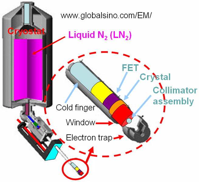
Overall, each absorbed X-ray photon generates a charge cloud that is composed of a number of electron-and-hole pairs, and the charge carriers are moved due to high voltage and are collected in the detector. The charge-sensitive preamplifier (PA) converts the charge pairs into a voltage pulse. The pulse is amplified and shaped in a spectroscopic amplifier (SPA). In this SPA process, one needs to optimize some constants such as gain, shaping time, pole zero, and base-line. The maximum of the intensified pulse is detected or stretched by peak-detector or peak-stretcher (PS). Finally, each pulse is individually measured with an analog-digital converter (ADC). The EDS detector can be integrated with a self-contained vacuum system (called a cryostat) as well as cryogenic pumping created by liquid nitrogen (LN2) cooling method as shown in Figure 4657b. The immersion lens (in-lens) acts as a perfect electron trap for the EDS detector without compromising the collection geometry of EDS or image resolution of SEM. Note that almost any materials in the detector window can attenuate the x-ray signal.
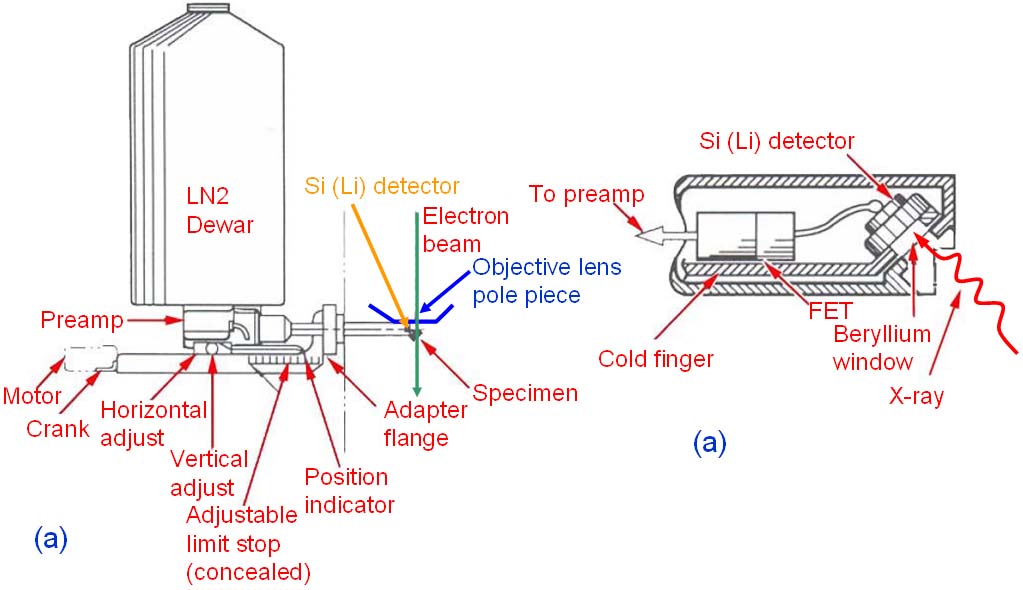
Figure 4657b. Schematic illustration of EDS detector. Figure 4657c shows the schematic illustration of a retractable EDS detector and its associated preamplifier electronics, and the detail of Si (Li) mounting assembly.
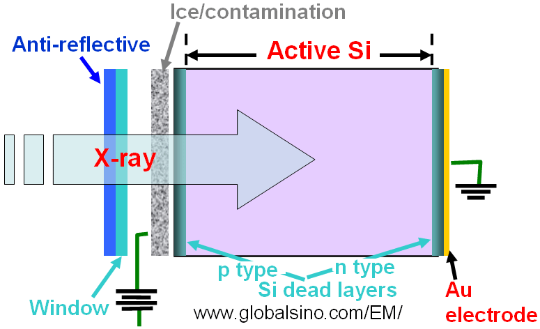
The main functions of the LN2 device (cryostat) are to reduce thermal e-h pair, prevent the Li atoms from diffusing, and reduce noise in the FET preamplifier. The “window” in Figure 4657b can be Be window in thickness of 7 to 12 µm, ultrathin polymer window in thickness of 100 nm, or windowless. Figure 4657d shows the structure of EDS detector. The anti-reflective layer can be an Al coating in thickness of 20 to 50 nm. The typical thickness of Au electrode is about 20 nm. The active Si can be an intrinsic silicon crystal in thickness of about 3 mm. The collector of e-h pairs is a reversed p-i-n structure. The Si dead layers are p-/n-type silicon crystal in thickness of about 100 nm. The existing dead layers also indicate that the generated charges cannot be completely detected.
Figure 4657d. Structure of EDS detector. Focusing X-ray optics has been used on both the excitation and detection sides in EDS systems. For instance, Gao et al. [1] suggested the use of polycapillary optics to provide an intense convergent beam of X-rays from a microfocus X-ray tube to excite the specimen for X-ray microfluorescence investigations. Wollman et al. [2] reported the use of a polycapillary optic to increase the effective area of their microcalorimeter EDS analysis. An intensity gain of ~300 (ratio of peak intensities with and without optic in place) was achieved in their case with a fixed detector-to-specimen distance of 66 mm. Von Harrach et al. [3] in FEI Company presented an advanced EDS detector for an FEI 200kV TEM/STEM system. In their system, the EDS detector, consisting of multiple windowless SDDs, had been integrated and placed symmetrically around the electron beam axis in the objective lens chamber without affecting the S/TEM resolution. The total active area of the SDDs was 120 mm2, designed by PN Sensor. The front-end electronics and ultra fast multi-channel pulse processor were provided by Bruker AXS MA. The processor was capable of fast mapping with pixel dwell times down to a few microseconds and >100 kcps count rates per channel. Furthermore, in many cases, electron traps are used to protect the EDS detectors in EMs as discussed in page2523. Comparing with side-entry specimen stages, top-entry specimen stages have better probe system parameters (e.g. Cs and Cc) and allow the X-ray spectrometers closer to the specimen. Note that there are considerable differences between various detectors from different companies. One detector may be better in one respect and another better in another respect.
[1] Gao N, Ponomarov I Y, Xiao Q F, Gibson W M, Carpenter D A (1996),
Monolithic polycapillary focusing optics and their application in microbeam
X-ray fluorescence. Appl Phys Lett 69:1529-1531.
|