=================================================================================
The intensities of the HAADF-STEM signals are sensitive to the crystal orientation through the electron-channeling phenomenon [1, 2]. In other words, at the major zone axes of the crystals in the specimen, the STEM probe may propagate preferentially down atom cores, resulting in stronger scattering to large angles than at ‘random’ orientations. Furthermore, the main result of multiple scattering in a STEM specimen is also that electrons can channel along the atomic columns. Especially, as high-resolution atomic column resolved images are taken with the electron beam travelling down the atomic columns, the channelling is unavoidable for most atomic-scale images. This channelling effect increases the effective depth of fields of the images. Note that the channeling effect induces the electrons in the probe to be periodically trapped by the attractive, periodic potential of the atoms in the crystal in the specimen. The process is similar to a fine waveguide. Due to the dynamical nature of the process the oscillating intensity of the electron wave on the atom sites with depth in the specimen is formed.
Haruta et al. [3] suggested that the channeling peak intensity at each atomic column not only depends on the type of atoms but also on the separation between the sub-columns of the same type of atoms. For instance, Figure 2797a (a) shows the double perovskite-rocksalt oxide La2CuSnO6 (LCSO) with Cu2+ and Sn4+ ions, determined by X-ray analysis, along b-axis projection. Figure 2797a (b) shows the atomic arrangement of La-b1, La-b2, and Sn along the b-axis projection. The electron beam of STEM is in the vertical direction. Figure 2797a (c) shows the channeling peak intensities at each La and Sn atomic column. Here, the intensities of La-b1 and La-b2 are different because the maximum intensity for each La was obtained at the center of a pair of La atomic columns in which the separation was too narrow to be resolved in the image. As shown in Figure 2797a (d), the electron-channeling peak intensity for La columns depends on the separations between La atoms as indicated by the two pairs of vertical lines in Figure 2797a (b).
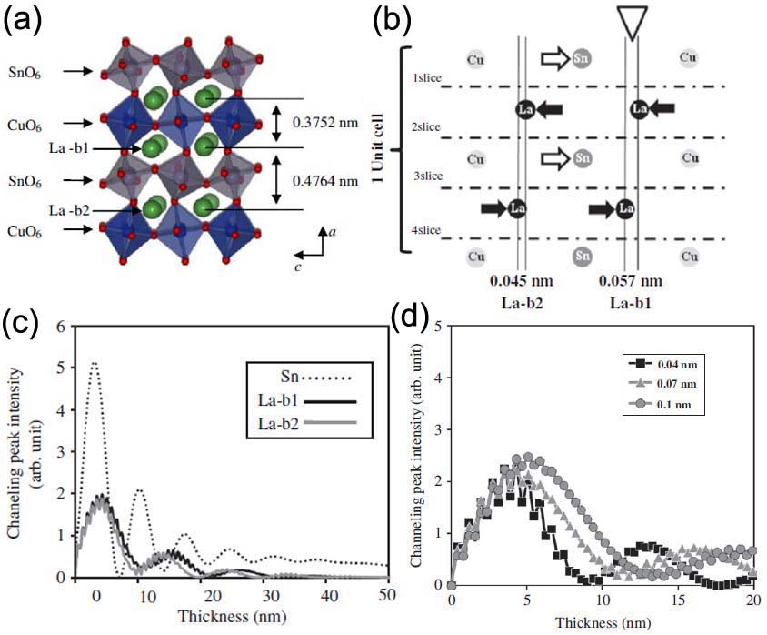
Figure 2797a. (a) Model of layered La2CuSnO6 along b-axis projection, (b) Cross-section along the b-axis projection (the electron beam is in the direction from the top to the bottom), (c) Simulated channeling peak intensity
at each atomic column in (b), and (d) Simulated electron-channeling peak intensity for La columns as a function of sample thickness for atomic column separations of 0.04 - 0.10 nm.
The simulations was performed by multislice method.
Adapted from [3].
On the other hand, a Cs-corrected probe has different channeling behaviour than a non-corrected probe as shown in Figure 2797b.
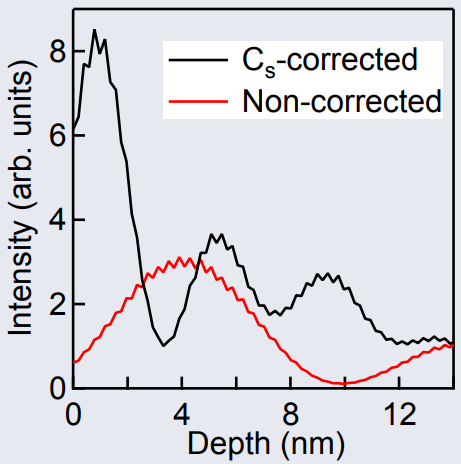
| Figure 2797b. Comparison between channeling behaviours of a Cs-corrected probe and a non-corrected probe. [4] |
[1] L. Fitting, S. Thiel, A. Schmehl, J. Mannhart, D.A. Muller, Ultramicroscopy 106
(2006) 1053.
[2] Z. Yu, D.A. Muller, J. Silcox, Ultramicroscopy 108 (2008) 494.
[3] M. Haruta, H. Kurata, H. Komatsu, Y. Shimakawa, S. Isoda, Effects of electron channeling in HAADF-STEM intensity in La2CuSnO6, Ultramicroscopy 109 (2009) 361–367.
[4] Susanne Stemmer,
Materials Department, University of California, Santa Barbara, USA, www.mrl.ucsb.edu.
|