
Chapter/Index: Introduction | A | B | C | D | E | F | G | H | I | J | K | L | M | N | O | P | Q | R | S | T | U | V | W | X | Y | Z | Appendix
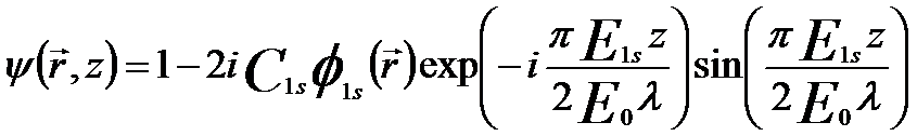
| In EM (electron microscopy) measurements, if the specimen is crystalline and aligned so that the electrons travel down a highly symmetric zone axis then the electrons will tend to be focused or channel down the atomic columns of the specimen. In this case, through the positive electrostatic potential of the atoms, a column acts as a channel for the electron, and thus the incident electrons can scatter dynamically without leaving the column. Electron channeling occurs if the incident beam is parallel to the atom columns of a crystal or a particular crystal defect. The channeling peak is of atomic dimensions and usually oscillates with depth in the specimen. [4 - 7] In a simplified channeling theory, an expression for the exit wave of a single atom column is expressed as [1 - 3], where, The S-state is the lowest energy bound state, which can be given by the Gaussian function, where, The width a depends on the energy of the S-state and is smaller for heavier atom columns and larger for weaker atom columns (normally 0.1 ~ 0.4 Å). In the aberration-free case, the intensity distribution resulting in the TEM images can be given by, The intensity distributes periodically with depth direction (z) even though the total intensity is conserved. The second term represents a non-linear contribution to the TEM images, while the third term represents a linear contribution. Figure 4152 shows the effects of a [100] oriented Si (silicon) lattice on a 100 keV incident plane wave, calculated using multislice method [9]. In this model, the electron beam is alternately transmitted through a thin slice and propagated to the next slice with a thickness of 1.3575 Å. During the propagation, the phase of the plane wave is shifted by the projected atomic potential. The peaks in the images correspond to the position of the atomic columns (channeling peaks). Note that there is a rapidly oscillating background in the electron wave intensity.
Figure 4152. Calculated electron intensity |ψ(r)|2 as the incident electrons pass through a [100] oriented Si lattice at depths of (a) 10 Å, (b) 100 Å, and (c) 200 Å. The positions labeled Si are the atom column positions.
Adapted from [10]
In the measurements based on STEM mode, the channeling effect is also sometimes called probe channeling. Note that there should be no channeling effect in any modes, including STEM and TEM modes, when the TEM specimen is only one-atom thick. Overall, the channeling effect depends on: Minimizing the channelling effect (dechannelling) can be achieved by:
[1] D.Van Dyck, H. Lichte, K. D. van der Mast, Sub-angstrom structure characterisation: the Brite–Euram route towards one angstrom, Ultramicroscopy 64 (1996) 1–15.
|
 ---------------------- [4152a]
 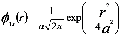 -------------------------------- [4152b]
 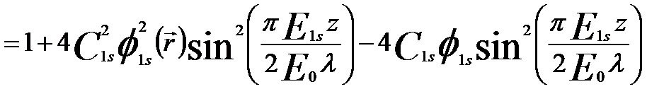 ----- [4152d]
 ![Calculated electron intensity |ψ(r)|2 as the incident electrons pass through a [100] oriented Si lattice at depths of (a) 10 Å, (b) 100 Å, and (c) 200 Å.](image1/4152dd.gif)