Table 3095a. P-3m1 (164) space group.
Name in the International Tables for Crystallography |
P-3m1 |
|
P |
|
164 |
|
-3m |
Crystal system |
Trigonal |
|
-3m |
Asymm |
0≤ x ≤ 2/3 and 0 ≤ y ≤ 1/3 and 0 ≤ z ≤ 1 and x ≤ (1+y)/2 and y ≤ x/2 |
|
12 |
Symmetry (atomic coordinates) |
Y, X, -Z; -Y, -X, Z; X-Y, -Y, -Z; -X+Y, Y, Z; -X, -X+Y, -Z; X, X-Y, Z.
X, Y, Z; -Y, X-Y, Z; -X+Y, -X, Z; X-Y, X, -Z; -X, -Y, -Z; Y, Y-X, -Z. |
Indices |
k, h, -l; -k, -h, l; h, -h-k, -l; -h, h+k, l; -h-k, k, -l; h+k, -k, l. |
Table 3095b. Examples of materials with P-3m1 (164) space group.
| |
Parameters |
Angles |
α = 90.0°; β = 90.0°; γ = 120.0° |
| |
Material |
Ba3NiNb2O9 [3] |
Lattice parameters |
a = b = 5.7550(5) Å; c = 7.0656(2) Å |
XRD pattern |
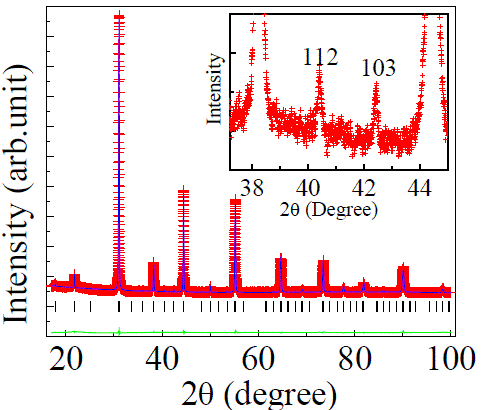
The (112) and (103) peaks in the inset indicates 1:2 ordering of B site ions (-Ni-Nb-Nb-) |
HAADF Z-contrast |
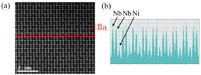
The intensities of the Nb and Ni atom columns in [010] direction shows the -Ni-Nb-Nb- ordering. Brightest contrast: Ba (Z=88); brighter contrast: Nb (Z = 73); weak contrast: Ni (Z=46). |
| |
Material |
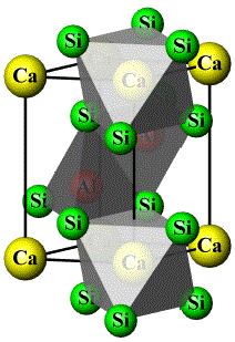
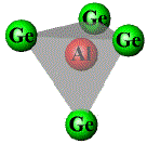
CaAl2Si2 [1] |
Structure with AlSi4 trigonal pyramids and CaSi6 trigonal
antiprisms (refer to MgAl2Ge2 below) |
 |
| |
Material |
K3Na(CrO4)2 |
Lattice parameters |
a = b = 5.858 Å; c = 7.523 Å |
| |
Material |
Mg(OH)2 |
Lattice parameters |
a = b = 3.1420 Å; c = 4.7660 Å |
| |
Material |
(K,Na)3Na(SO4)2 (aphthitalite) |
Lattice parameters |
a = b = 5.68 Å; c = 7.31 Å |
| |
Material |
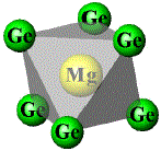
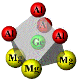
MgAl2Ge2 [1] |
Lattice parameters |
a = b = 4.11693(5) Å; c = 6.7873(1) Å |
Cell volume V |
99.627(3) Å3 |
Atomic coordinates |
Mg: Wyckoff position = 1a, x = 0, y = 0, z = 0; Al: Wyckoff position = 2d, x = ⅓, y = ⅔, z = 0.6353(3); Ge: Wyckoff position = 2d, x = ⅓, y = ⅔, z = 0.2419(2) |
Interatomic distances and coordination polyhedra |
| Atoms |
|
δ (Å) |
Polyhedron |
| Mg |
-6 Ge |
2.8888(8) |
 |
| Al |
-3 Ge
-1 Ge |
2.5188(8)
2.6701(24) |
 |
| Ge |
-3 Al
-1 Al
-3 Mg |
2.5188(8)
2.6701(24)
2.8888(8) |
 |
|
| |
Material |
α-Zr2N2S [2] |
Lattice parameters |
a = b = 3.605(2) Å; c = 6.412(3) Å |
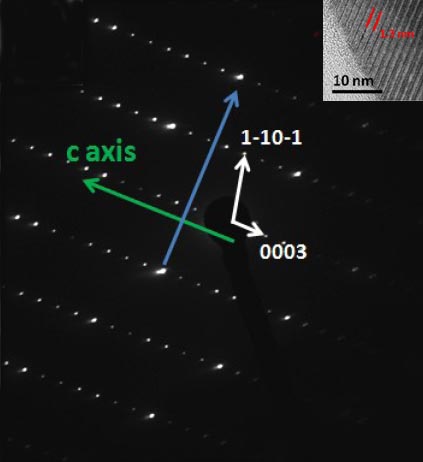
HRTEM |
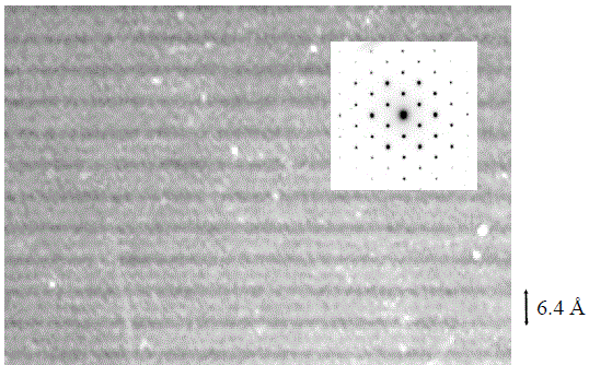
Inset: 0 0 1 zone axis electron diffraction pattern in hexagonal symmetry without superstructure reflections |
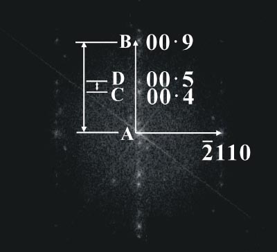
For hcp crystals, the (0 0 0 l) reflections, e.g. for the case with 164 (P-3m1) space group, are forbidden when l is odd. However, those reflection positions often show diffraction intensity, which is probably caused by chemical order on the basal planes, or by double or multiple diffraction (scattering).
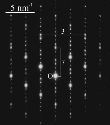
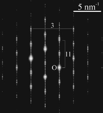
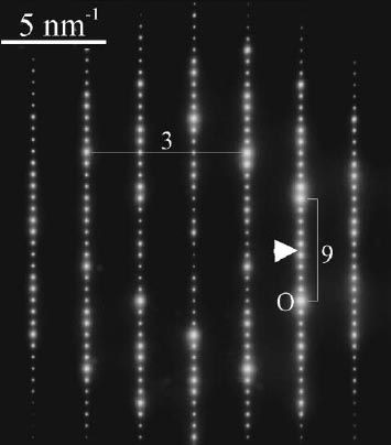
For [0 1 -1 0] Sb3Te2 in Figure 3095a, the ratio of AB/CD is the layer number (N) in a unit cell. We can know the Sb3Te2 crystal belongs to the P-3m1 space group as N is 9, a multiple of 3. Note that we can index diffraction patterns starting from comparing experimental d-spacings and theoretical calculations obtained from known lattice parameters, for instance, use the excel file for crystals with P-3m1 space group.
|
|
|
[0001] η-phase Cu3Si [7]
(a = 4.06Å and c = 7.33Å) |
|
|
|
|
|
[0 1 -1 0] Ge2Bi2Te5. [4] |
[0 1 -1 0] Sb3Te2. [4] |
|
|
|
|
[-1 2 -1 0] Ge2Bi2Te5. [4] |
[2 -1 -1 0] Ge2Bi2Te5
(space group p-3m1) [4] |
[2 -1 -1 0] Ge2Bi2Te5. [4] |
|
|
|
[1 1 -2 0] Ge1Sb2Te4. [5] |
[1 1 -2 0] Ge1Sb2Te4. [6]
(a' = 0.425 nm and c' = 4.10 nm) |
[1 1 -2 0] Ge3Sb2Te6. [6]
(a' = 0.425 nm and c' = 6.26 nm) |
|
|
|
[1 1 -2 0] Ge2Sb2Te5. [6]
(a' = 0.425 nm and c' = 1.827 nm) |
|
|
|
|
|
[3 -3 0 1] η-phase Cu3Si [7]
(a = 4.06Å and c = 7.33Å) |
|
|
|
|
|
[1 4 -11 1] Ge2Bi2Te5. [4] |
[1 0 -10 -1] Ge2Bi2Te5. [4] |
|
Figure 3095a. Examples of indexed electron diffraction (or FFT) patterns of 164 (P-3m1) HCP crystals.
[1] Svitlana Pukas, Liliya Pylypchak, Oksana Matselko, Pavlo Demchenko, Roman Gladyshevskii, MgAl2Ge2 – a new representative of the structure type CaAl2Si2, Chem. Met. Alloys 5 (2012) 59-65.
[2] Chad Alan Stoltz, Synthesis of Layered Group IV Nitride Materials by Soft Chemical Anion Metathesis, thesis, 2005.
[3] Jungmin Hwang, Magnetoelectric and Multiferroic Properties in Layered 3d Transition Metal Oxides, thesis, 2012.
[4] Chang Woo Sun, A Transmission Electron Microscopy Study on the Microstructural Properties of Te-based Chalcogenide Thin Films, Doctoral Thesis, 2010.
[5] Enzo Rotunno, Advanced analytical transmission electron microscopy methodologies for the study of the chemical and physical properties of semiconducting nanostructures, Doctoral Thesis, 2014.
[6] B. J. Kooi and J. Th. M. De Hosson, Electron diffraction and high-resolution transmission electron microscopy of the high temperature crystal structures of GexSb2Te3+x (x = 1, 2, 3
) phase change material, J. Appl. Phys.92 (7), 3584 (2002).
[7] Cheng-Yen Wen & Frans Spaepen, In-situ electron microscopy of the phases of Cu3Si, Philosophical Magazine, 87(35), 5581-5599, 2007.
|
![[0001] η-phase Cu3Si](http://www.globalsino.com/EM/image2/3095abc.gif)
![[0 1 -1 0] Ge2Bi2Te5](image2/3040g.jpg)
![[-1 2 -1 0] Ge2Bi2Te5](image2/3040j.jpg)
![[2 -1 -1 0] Ge2Bi2Te5](image2/3040e.jpg)
![[2 -1 -1 0] Ge2Bi2Te5](image2/3040f.jpg)
![[3 -3 0 1] η-phase Cu3Si](http://www.globalsino.com/EM/image2/3040ii.gif)
![[1 4 -11 1] Ge2Bi2Te5](image2/3040h.jpg)
![[1 0 -10 -1] Ge2Bi2Te5](image2/3040i.jpg)