Chemical Shift Detection of Elements by EELS and EFTEM - Practical Electron Microscopy and Database - - An Online Book - |
|||||
| Microanalysis | EM Book http://www.globalsino.com/EM/ | |||||
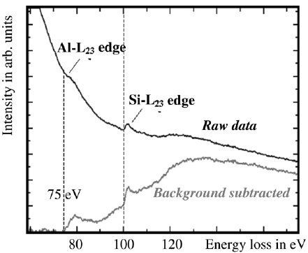
The EEL spectra in Figure 3385a show the Al L2,3 edge as well as the Si L2,3 edge after background subtraction, taken from AlxSiyOz matrix. The threshold value of the Al ionization edge here is about 75 eV indicating that aluminum is bonded to oxygen because the onset energy of the edge of pure aluminum is about 73 eV. This energy difference is called chemical shift. In general, due to the chemical shifts, the edge energies provided in literature (e.g. the Periodic Table) are only accurate to -2 eV ~ + 7 eV.
Figure 3385a. EELS profile of Al and Si taken from AlxSiyOz matrix by a electron probe of 2 nm in diameter. [1]
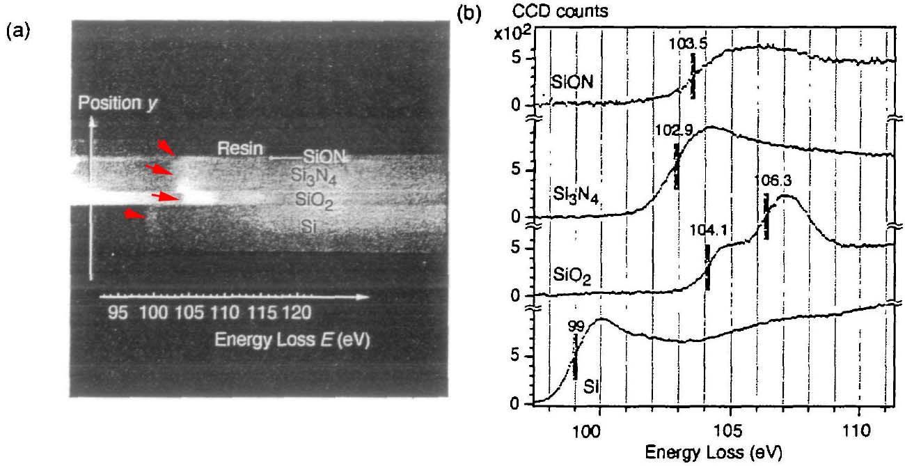
The L3 edge for a specific 3d transition metal exhibits a chemical shift toward higher energy losses with an increase in oxidation state. ELNES mapping is enabled by the fact that chemical bonding and short-range order in the environment of a specific chemical element induce a chemical shift of the energy-loss edge in the range between 0.1 and 8 eV and modifies the near-edge fine structure (ELNES) of the electron energy-loss spectrum. Therefore this method can differentiate between compounds of the same binary or multi-component system but with different bonding and valency. The chemical shift can be mapped by narrow energy slits. For instance, depending on the environment of Si element, the chemical shift of Si L2,3 energy loss edge can be up to 6.9 eV. Therefore, the resulting chemical shift can be mapped using the energy filtered imaging taken with a narrow energy slit of 1.8 eV or similar spectrum mapping in STEM mode. To find optimal settings for chemical shift analysis, if EFTEM mode is employed a series of energy-filtered images should be taken near the edge energy with a small energy step. For instance, Kimoto et al [2] observed 27 energy-filtered images near the Si L2,3 edge energy (99 eV) with a 1.0 eV energy step. Figure 3385b shows that the chemical shifts are revealed by spatially resolved EELS of Si-L2,3 edges. Figure 3385b (a) shows the 2-D (two-dimensional) spectrum image obtained by an energy filter. Note that this image shows the image contrast before background subtraction. The vertical axis corresponds to the location (y) in the layered materials of SiON. Si3N4, SiO2 and pure Si. The horizontal axis corresponds to the energy loss E. For chemical shift analysis, small energy dispersions, e.g. 0.051 eV per pixel here, are normally used. The energy range ΔE recorded in the 2-D spectrum image was 52 eV (= 88 - 141 eV in energy loss). Both the shift of the bright lines (shown by red arrows) in Figure 3385b (a) and the vertical lines in Figure 3385b (b) indicate the chemical shift of Si-L2,3 edges. Figure 3385b (b) shows energy loss spectra of each layer extracted from Figure 3385b (a). Here, the backgrounds of the spectra were subtracted.
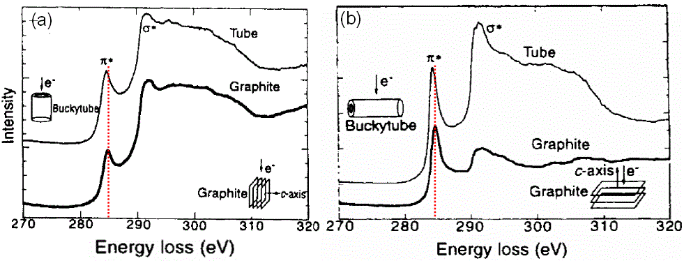
Figure 3385b. The spatially resolved EELS analysis of Si-L2,3 edges, (a) 2-D spectrum For carbon nanotubes and graphite, as shown in Figure 3385c, not only does the core electron EELS spectra for the nanotubes shift to lower energies from those of graphite due to their lower-dimensional feature and thus due to the lower carrier densities and conductivities than graphite, but also the EELS on both the tubule bundle and graphite are sensitive to the incident electron beam along their crystalline axis.
Figure 3385c. Core electron EELS spectra for both nanotubes and graphite with the incident electron in TEM along their different crystal orientations.
Adapted from [5]
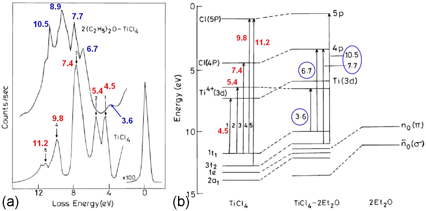
Figure 3385d shows the EELS recorded with a home-built spectrometer [3], and the energy level diagram and electronic transitions of TiCl4 and TiCl4-2Et2O complex. For TiCl4, there are five prominent peaks 1 to 5 (in red). The first peak at 4.5 eV originates from the transition 1t1 to e, while the second one at 5.4 eV is due to the transition 1t1 to 1t2. The intense peak at 7.4 eV originates from the Rydberg transition 1t1 to 4P. The features at 9.8 and 11.2 eV originate from the transitions from the 1t1 and 3t2 orbitals to the Cl(5P) level. The spectrum of the TiCl4-2Et2O complex has the transitions at 3.6, 6.7, 7.7, 8.9, and 10.5 eV (in blue). The first peak at 3.6 eV originates from the charge transfer band due to the transition from the highest occupied shifted chlorine lone pair orbital to the Ti4+(3d). The peaks at 6.7 and 7.7 eV are from the transitions from the shifted 1t1 and 3t2 chlorine orbitals to the 4p Rydberg states. This shift is due to the complex formation. The peak at 10.5 eV originates from the 3t2 to 5p transition. Therefore, when the tetrahedral TiCl4 molecule is bonded to form octahedral TiCl4-2Et2O, the molecule should become more ionic. [4] The charge-transfer band in TiCl4 at 4.5 eV is shifted to 3.6 eV because of the change in the electronic structure of the molecule.
|
|
||||