| Manufacturers have attempted to use van de Graaff generators to supply high voltages to TEM systems, but the favorite voltage source is still Cockcroft–Walton voltage generator.
The high-voltage generated with a high-voltage generator (e.g. Cockcroft–Walton voltage generator) is supplied to acceleration tube through the high voltage cable of electron microscopes, and thus the electrons are accelerated in the acceleration tube. In TEM systems, a multi-stage acceleration electrode is used as shown in Figures 1967a and 1967b. The accelerator tube is composed of a stack of porcelain insulators sealed together by metal flanges and O rings. The accelerating electrodes are usually made of highly polished metal.

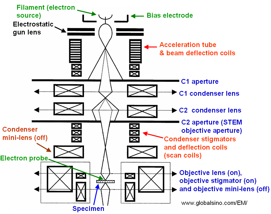
| Figure 1967a. Schematic illustration of the probe-forming electron optics in STEM mode in JEOL JEM-2010F TEMs. |
For convenience of microscope operation, we need to consider the coupling between the accelerator and the condenser system. The input electron beam to the condenser system should not vary significantly as the working voltage is changed. The position of the crossover of the beam leaving the accelerator especially should not move greatly along the axis.
The schematic illustration in Figure 1967b presents the position of acceleration tube in typical TEM systems.
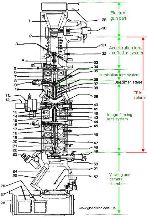
 |
1. Electron gun
2. Wehnelt unit
3. Anode
4. Electron gun second beam delector coil
5. Anode chamber isolation valve
6. 1st condenser lens coil
7. Condenser polepiece
8. 3rd condenser lens coil
9. Condenser aperture assembly
10. Specimen chamber
11. Goniometer
12. specimen holder
13. Stigmator screening cylinder
14. Objective lens coil
15. Objective lens liner tube
16. Field limiting aperture
17. Intermediate lens stigmator
18. Intermediate polepiece
19. Intermediate lens linear tube
20. Projector lens beam deflector coil
21. Projector upper polepiece
22. Projector lower polepiece
23. Binoculars
24. Viewing chamber
25. Viewing window
26. Dispensing magazine
27. Receiving magazine
28. Camera chamber
29. Lift arm
30. HT cable to high voltage tank
31. Anode chamber, or called acceleration tube
32. Gas inlet
33. Electron gun 1st beam deflector coil
34. Condenser lens stigmator coil
35. Spot alignment coil
36. Condenser lens 1st beam deflector coil
37. Condenser lens 2nd beam deflector coil
38. Condenser minilens (CM) lens coil
39. Stage heater
40. Objective polepiece
41. Objective lens stigmator coil
42. 1st image shift coil
43. Objective minilens (OM) lens coil
44. 2nd image shift coil
45. 1st intermediate lens coil
46. 2nd intermediate lens coil
47. 3rd intermediate lens coil
48. Projector lens coil
49. Viewing chamber isolation valve
50. High resolution diffraction chamber
51. Small screen
52. Large screen |
Figure 1967b. Schematic illustration of the structure of typical TEM systems (e.g. JEM-2010F
here). |
The output of Cockcroft–Walton voltage generator is then connected to the electrode stages in the accelerator tube as shown in Figure 1967c. Each electrode stage is powered by a divided voltage supplied through the bleeder resistors that are connected to the output of the voltage generator. In the case that the high voltage is higher than several hundred kV, more than 15 stages of acceleration electrodes are often employed.

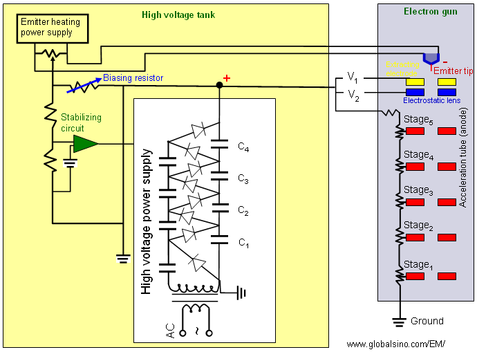
Figure 1967c. Electronic connection between Cockcroft–Walton voltage generator and accelerator tub in TEMs.
Such voltage generators may be either air-insulated or confined in a tank filled with an insulating gas (e.g. freon, nitrogen, SF6) under pressure. For such systems, a large room or even a separate building is required to provide enough clearance against spark-over. Note that some systems have both generator and accelerator in a common tank; others use two separate tanks to minimize electrical interaction and make the service more convenient.
The design best-known methods (BKMs) for accelerating voltage in Scanning Electron Microscopy (SEM) and Transmission Electron Microscopy (TEM) are important for controlling the electron beam's interaction with the sample, influencing imaging resolution, depth of penetration, and signal generation.
SEM Accelerating Voltage Design Best-Known Methods:
- Variable Accelerating Voltage Control: SEMs typically allow for a wide range of accelerating voltages, usually between 0.5 kV to 30 kV. This flexibility enables users to adjust voltage depending on the application:
- Low voltage (0.5–5 kV): Minimizes beam penetration and charging for surface-sensitive imaging, ideal for non-conductive or biological samples.
- High voltage (15–30 kV): Provides greater penetration, ideal for thicker or denser materials, and enhances backscattered electron (BSE) signal for compositional contrast.
- Field Emission Gun (FEG) Designs: For high-resolution imaging at low accelerating voltages, field emission sources (e.g., Schottky or cold FEG) are used. These electron guns provide a bright, coherent electron beam, improving resolution at lower voltages, particularly important for delicate or beam-sensitive samples.
- Optimized Electron Optics: Electron lenses and stigmators in SEMs are optimized to maintain focus and minimize aberrations at different accelerating voltages. This helps provide clear images across the range of voltages without significant beam divergence or distortion.
Dynamic Beam Control: Advanced SEM systems may feature dynamic focusing and astigmatism correction that automatically adjusts based on the selected accelerating voltage. This ensures consistent image quality and depth of field at different voltages.
- Voltage Range Selection for Specific Applications:
- Low-voltage imaging for surface detail: Using <1 kV to 2 kV is a BKM for minimizing sample charging and enhancing surface detail in biological or non-conductive materials.
- High-voltage for deeper imaging and element mapping: High voltages (20–30 kV) are preferred for applications like energy dispersive X-ray spectroscopy (EDS), where greater penetration and excitation are needed to generate characteristic X-rays.
- Stage Biasing Techniques: To effectively reduce sample charging, particularly for low-voltage SEM, some designs include stage biasing (applying a small voltage to the stage) to neutralize the sample and maintain clear images at lower accelerating voltages.
TEM Accelerating Voltage Design Best-Known Methods:
- High Voltage Operation (100–300 kV): TEMs operate at higher accelerating voltages, typically ranging from 80 kV to 300 kV. Higher voltages provide:
- Higher Resolution: Higher accelerating voltage reduces electron wavelength, which improves the resolution and enables atomic-level imaging, particularly in high-resolution TEM (HRTEM).
- Deeper Penetration: Higher voltage allows the electron beam to penetrate thicker samples, which is essential for studying internal structures in materials and biological specimens.
- Adjustable Accelerating Voltage: In many modern TEMs, the accelerating voltage is adjustable depending on the sample and the technique:
- Low voltage (60–100 kV): Useful for beam-sensitive materials (e.g., biological samples or soft polymers) to minimize damage.
- High voltage (200–300 kV): Preferred for materials science applications where high resolution, deep penetration, and reduced scattering effects are necessary.
- High-Tension Supply Stability: Ensuring a stable and precise high-tension (HT) supply is critical in TEMs to maintain consistent accelerating voltage. This reduces fluctuations in beam energy, which could otherwise degrade resolution and cause imaging artifacts.
- Optimized Column and Lens Design: The electron optical column and lenses in TEM are specifically designed to handle the high accelerating voltages while minimizing spherical and chromatic aberrations. This allows for precise focusing and improved resolution, especially at voltages above 200 kV.
- Corrector Technology for Aberrations: In high-end TEMs, aberration-corrected lenses are often used to compensate for the inherent optical aberrations that occur at higher accelerating voltages. This enables atomic-resolution imaging even at voltages around 200–300 kV.
- Multi-mode Voltage Operation: Some TEM systems are designed with multi-mode operation, allowing users to switch between high-voltage TEM mode for deep penetration and high-resolution imaging, and low-voltage mode for studying beam-sensitive materials.
- Specialized Techniques Based on Accelerating Voltage:
- Cryo-TEM at Low Voltage: For biological cryo-TEM, lower voltages (e.g., 80 kV) are often used to reduce radiation damage while maintaining structural integrity in frozen samples.
- High Voltage TEM for Defect and Dislocation Studies: In materials science, high-voltage TEM (up to 300 kV) is used to examine dislocations, grain boundaries, and other defects within crystalline materials.
|