
Chapter/Index: Introduction | A | B | C | D | E | F | G | H | I | J | K | L | M | N | O | P | Q | R | S | T | U | V | W | X | Y | Z | Appendix
| Table 2074a. Properties of silicon nitrides.
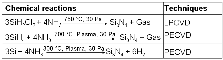
Table 2074b. Chemical reactions used in CVD for Si3N4 film growth.
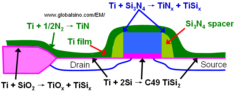
* LPCVD: low pressure CVD; PECVD: plasma-enhanced CVD. Figure 2074 shows several chemical reactions occurring during annealing of a transistor structure coated with Ti to form a low resistive TiSi2 layer at the source, gate, and drain. When silicon and titanium are reacted, Ti and Si can diffuse laterally over the isolation regions and form thin filaments of TiSix that can electronically connect a gate electrode and source/drain regions and can cause failure of the device. This phenomenon is called "bridging". On the other hand, those by-products (TiSix, TiOx, and TiN) form over the isolation regions and cannot easily be etched in conventional salicide etching solutions. The use of a nitrogen atmosphere during thermal annealing is essential in preventing this failure mechanism [1] because nitrogen quickly diffuses into the grain boundaries and significantly suppresses any long-range silicon diffusion in the titanium layer. Furthermore, to avoid the by-product formation, the annealing temperature cannot be too high.
Figure 2074. Several chemical reactions occurring during annealing of a transistor structure coated with Ti to form a low resistive SiTi2 layer. Some phenomena related to Si3N4 are important in ICs. For instance, evidences show that the Cu/Si3N4 cap interface is the dominant electromigration path, [2,3]. In EELS, the silicon ‘metallic’ bulk plasmon is found at 17 eV, and it moves up to 23 eV for silicon nitride (Si3N4). Table 2074c. Etchants used in semiconductor manufacturing.
Table 2074d. Etching selectivity of Si3N4:SiO2:Si in various solutions.
Table 2074e. Color chart for Si3N4 films observed perpendicularly under daylight fluorescent lighting.
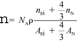
The density (n) of valence electrons in Si3N4 is given by, As discussed in page3417, the plasmon energy of a material is determined by the density (n) of valence electrons in the material. For SiNx, the plasmon energy decreases with the increase of excess silicon concentration, which can be explained by, The atomic density of SiNx materials decreases from 3.0 g/cm3 (for Si3N4) to 2.33 g/cm3 (for Si).
[1] C. K. Lau, “Method of Forming Titanium Disilicide,”
U.S. Patent 4,545,116, 1985.
|
||||||||||||||||||||||||||||||||||||||||||||||||||||||||||||||||||||||||||||||||||||||||||||||||||||||||||||||||||||||||||||||||||||||||||||||||||||||||||||||||||||||||||
 ------------------------- [2074a]
 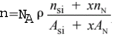 ------------------------- [2074b]