=================================================================================
The TEM specimen thickness (t) can be determined by off-axis electron holography,
 ------------------------------------ [2551] ------------------------------------ [2551]
where,
CE -- The interaction constant between the fast electrons and matter, dependent on the energy of the electron wave (e.g. 7.29 x 10⁻³ rad V−1 nm−1 for 200 kV electrons),
V0 -- The electrostatic potential, or called the mean inner potential (MIP in V),
Δϕ -- The change in phase of an electron as it passes through the TEM specimen.
If V0 is known, then t can be determined by Δϕ that is obtained by reconstruction of holograms.
Two-dimensional (2-D) maps of electron phase shifts reconstructed from off-axis electron holograms can be used to quantify the thickness of materials. Zheng et al. had used this technique to investigate the thickness (height) of (Si,Ge) islands on Si (silicon) substrates. To avoid diffraction-induced artifacts, the electron hologram was recorded under weak diffraction conditions by tilting the specimen several degrees away from [001] zone axis. The islands presented in Figure 2551 (a) were covered by the fine biprism fringes, while the vacuum area at the bottom of the image was used as a reference. The inset in Figure 2551 (a) shows the magnified image of the selected region in the white frame. The strong distortion of the fringes across the island in the magnified image indicates large phase shifts of the electrons due to the thickness variation across the island. The reconstructed amplitude map shown in Figure 2551 (b) looks like a conventional BF (bright-field)-TEM image with less details of the features, but more noisy than in BF-TEM image. The bright contrast shown in the islands in Figure 2551 (c) reveals the large phase difference between the islands and the Si substrate because of the different thickness. Figure 2551 (d) shows a magnified portion of the phase image in Figure 2551 (c). The phase spacing between two adjacent black or white lines is ~0.2 π. Each island contains a set of highly dense, square-shaped contour lines. The density of the contour lines indicates the variation of the height in the islands.
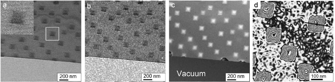
Figure 2551. (a) Electron hologram of (Si,Ge) islands on a (001) Si substrate. The inset shows the magnified image of the selected region in the white frame. (b) The reconstructed amplitude image. (c) The unwrapped phase image. (d) The magnified phase image of islands on the Si substrate. Adapted from [1]
[1] C. L. Zheng, K. Scheerschmidt, H. Kirmse, I. Häusler, W. Neumann, Imaging of three-dimensional (Si,Ge) nanostructures by off-axis electron holography, Ultramicroscopy 124 (2013) 108–116.
|