|
This book (Practical Electron Microscopy and Database) is a reference for TEM and SEM students, operators, engineers, technicians, managers, and researchers.
|
=================================================================================
The grains in Cu interconnects in ICs normally span the entire linewidth at linewidths of less than 2 µm (called bamboolike microstructure). In this case, Cu in electromigration (EM) processes migrates at the interface between Cu and the dielectric diffusion barrier because these grains act as blocking grains. However, no blocking grain exists in the linewidths of 4–6 µm (the Cu microstructure is in polycrystalline phase). In this case, Grain boundary and/or interface diffusion can occur in the EM process. SIM images in Figure 2902 show the microstructures of the Cu interconnects with Ta liner: (a) Cu linewidth of 0.8 µm (bamboolike microstructure), and (b) Cu linewidth of 6 µm (polycrystalline). Note that the Ea of grain-boundary diffusion of electroplated Cu is 1.08 eV. [2]
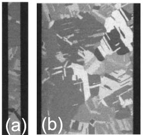
Figure 2902. SIM images of the Cu interconnects with Ta liner: (a) Cu linewidth of 0.8 µm (bamboolike microstructure), and (b) Cu linewidth of 6 µm (polycrystalline).
Adapted from [1]
In the grain boundary diffusion mechanism of electromigration, the electromigration process is retarded if the grain sizes are too small. For instance, the increased time to failure of Al-4 wt. % Cu alloy over pure Al in electromigration [3] can be explained by the difference of grain growth rates. In Al-4 wt. % Cu alloy, the grains are initially small and thus the ions remain essentially immobile to migration, resulting in enhanced component life.
[1] T. Usui, H. Nasu, T. Watanabe, H. Shibata, T. Oki, and M. Hatano, Electromigration diffusion mechanism of electroplated copper and cold/hot two-step sputter-deposited aluminum-0.5-wt% copper damascene interconnects, Journal of Applied Physics 98, 063509 (2005).
[2] D. Gan, P. S. Ho, R. Huang, J. Leu, J. Maiz, and T. Scherban, J. Appl.
Phys. 97, 103531 (2005).
[3] William C. Mcbee, and John A. Mccomb, Grain Growth in Thin Aluminum-4% Copper Alloy Films, Thin Solid Films, 30 (1975) 137-143.
|