Dead Layers in EDS Detector - Practical Electron Microscopy and Database - - An Online Book - |
|||||
| Microanalysis | EM Book https://www.globalsino.com/EM/ | |||||
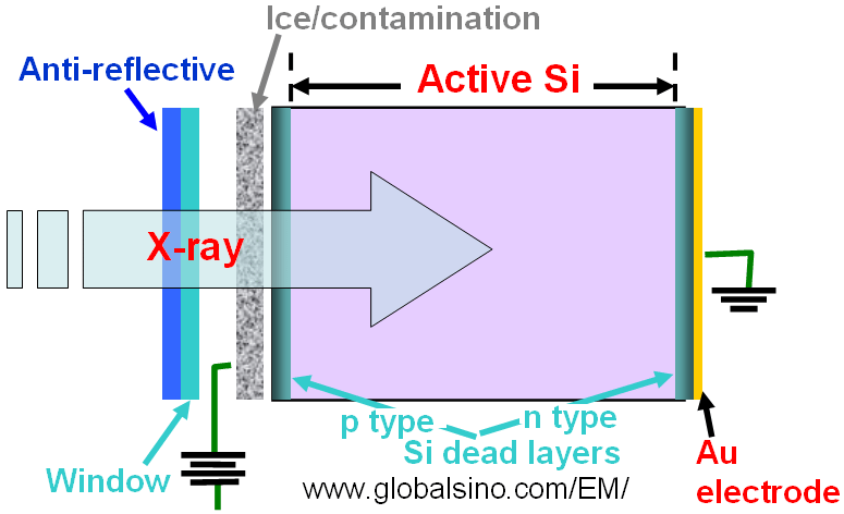
Figure 3806a shows the structure of EDS detector. The active Si can be an intrinsic silicon crystal in thickness of about 3 mm. The collector of e-h pairs is a reversed p-i-n structure. The Si dead layers are p-/n-type silicon crystal in thickness of about 100 nm. The existing dead layers also indicate that the generated charges cannot be completely detected.
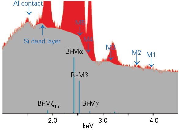
Figure 3806a. Structure of EDS detector. Figure 3806b shows the EDX spectrum of bismuth (Bi). The bremsstrahlung background in grey was obtained by physical modeling. In the spectrum, the absorption edges of the X-ray lines of the elements (Al contact, Si dead layer) on the detector surface are also visible.
Figure 3806b. EDX spectrum of bismuth (Bi). [1]
[1] QUANTAX, EDS Analysis for SEM and TEM, Bruker.
|
|
||||