=================================================================================
This broadening disadvantage does not exist in conventional STEM-based EELS. The spatial resolution of EELS measurements in modern STEMs is between 0.1 and 1 nm.
The spatial resolutions of EFTEM can be slightly worse than those of HAADF and TEM imagings primarily due to the specimen drifts during the slower acquisitions of the spectra or elemental mapping. On the other hand, the spatial resolution in EFTEM is improved with the accelerating voltages, since the incident electron beam broadening (spread) decreases with an increase of the voltage.
In EFTEM imaging, other important contribution for low-loss imaging is the delocalization of the inelastic scattering process itself, while at much higher energy-losses the resolution-limiting parameter is usually the chromatic aberration. For instance, to lower the effect of the chromatic aberration, the accelerating voltage needs to be 300 kV if one expects a resolution better than 0.3 nm for >100 eV energy-loss [1].
Figure 3820 shows the typical sizes of various material defects and the capability of analytical techniques (See the full names of the techniques at page3928). The lowest levels of the techniques represent their spatial resolutions.
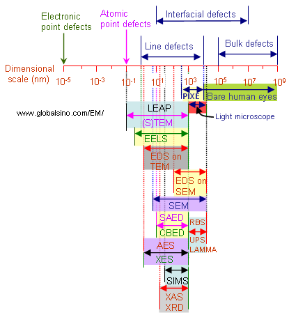
Figure 3820. Typical sizes of various material defects and capability of analytical techniques.
[1] R.F. Egerton, Electron Energy-Loss Spectroscopy in the
Electron Microscope, 2nd Edition, Plenum Press, New
York, 1996.
|