=================================================================================
Figure 3855 shows the PVC (passive voltage contrast) in the contact level of WL (word line) decoder of a DRAM circuit. The gate contacts generate dark signal because they are fully positively charged. The p-contacts in n-well and n-/p- well contacts generate the brightest signal. The n-contacts in p-well generate the second brightest signal.
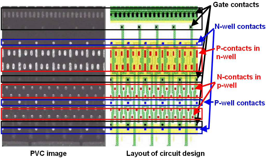
Figure 3855. The PVC in contact level of WL (word line) decoder of a DRAM circuit. Adapted from [1].
If a gate structure in MOS transistors or the structure which is connected to the gate is relatively large, they should be considered as a capacitor. Therefore, the duration which the gate or connected structure is exposed to the incident beam in FIB or SEM can be too short so that they are not significantly charged to affect their PVC.
[1] Ruediger Rosenkranz, Failure localization with active and passive voltage contrast in FIB and SEM, J Mater Sci: Mater Electron (2011) 22:1523–1535.
|