=================================================================================
The number of diffraction spots showing on the screen or detector in TEM depends mainly on the accelerating voltage of the incident electrons, the alignment of the thin film relative to the optical axis, the film thickness, and the beam convergence.
For instance, in the case of thin TEM films, the relaxation of the Bragg conditions occurs at the reciprocal lattice points. Those reflection (diffraction) points are transformed into relrods elongated normal to the TEM film as shown in Figure 3908. This is also the reason why reflection spots are always shown in the electron diffraction pattern (EDP) even though the "perfect" Bragg condition sometimes is not exactly satisfied. Since this elongation is inversely proportional to the specimen thickness (t), the relrods become very elongated for very thin TEM films so that many of them can simultaneously intersect the Ewald sphere and produce diffracted beams. The number of the shown diffraction spots on the TEM screen or detector is more than that from a thick TEM film.
Similar to the case of “single-electron beam” tilt in TEM, with a convergent incident beam (Convergent Beam Electron Diffraction, CBED) we can split the beam into many electron rays, which are smaller electron beams C1 to Cn shown in Figure 3910. Each incident ray inside the incident beam has a different Ewald sphere because it has a different ray orientation. All those Ewald spheres locate between the two extreme spheres ‘‘-α’’ and ‘‘+α’’. Differently intersecting the same relrod by different Ewald sphere gives different excitation error (s). Each reciprocal lattice point located between these two extreme spheres gives a diffracted intensity. One application of CBED is, therefore, a large convergence at a semi-angle α can be very useful to obtain a large number of reflections.
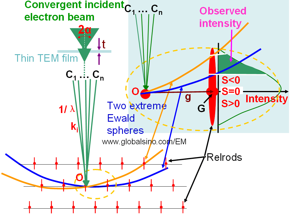
Figure 3910. Ewald sphere construction with a convergent incident electron beam on a thin TEM film.
The dotted line along the electron beam indicates the beam path through lenses.
The Precession electron diffraction (PED) patterns not only display more diffraction spots in the zero-order Laue zone (ZOLZ) than SAED ( selected-area electron diffraction) and NBED (nanobeam electron diffraction) but also show some diffraction spots in the high-order Laue zones (HOLZ) which normally do not show in SAED and NBED patterns. PED also can show more diffraction spots than the conventional diffraction techniques.
|