=================================================================================
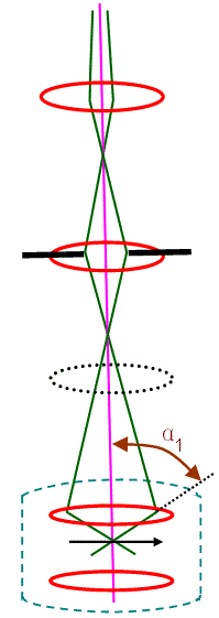
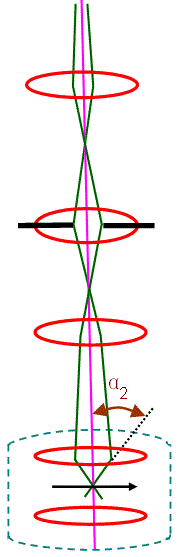
The probe formation in CBED measurement is different from other TEM modes. The schematic illustrations in Figure 4144 show the convergent illumination configurations of various modes in TEMs. In the CTEM condition in Figure 4144 (a), the condenser mini-lens (CM lens) is strongly excited, and incident electrons are focused on the pre-focal point of the objective pre-field, resulting in a parallel illumination on a wide area on the specimen and providing highly coherent electron illumination. In the EDS condition in Figure 4144 (b), the CM lens is turned off and the incident electrons are focused on the specimen by the objective pre-field, resulting in a small-probe illumination. In this case, the illumination angle (α1) is large so that high beam intensity is obtained for a small area in the analytical EDS method. In the NBD mode in Figure 4144 (c), a smaller condenser aperture is used to form a smaller illumination angle (α2). Therefore, a small-diameter probe with relatively high coherence in the illumination is achieved. In the illumination condition in Figure 4144 (c), the illumination angle (α) with a constant probe size can be changed by changing the excitations of the condenser lenses and the CM lens to obtain the incident illumination to form ideal convergent beam electron diffraction (CBED) patterns.
Figure 4144. Convergent illumination configurations: (a) CTEM mode, (b) EDS mode and (c) NBD mode.
Convergent-beam electron diffraction (CBED) and large-angle CBED is generated by a cone of primary electrons. Historically, CBED is the oldest TEM diffraction technique.
A convergent beam of electrons can limit the illuminating region of the specimen which contributes to the diffraction pattern, so that it provides structural information from small specimen regions. In other words, CBED patterns are produced by focusing the electron beam to crossover in the specimen plane. This region is a function of the beam size and beam-specimen interaction volume, which increases with specimen thickness but can be much smaller than in SAD (selected area diffraction). The incident beam in CBED can be considered as made of a set of incident rays, within an incident cone, relative to many crystalline orientations.
In SAD, the electron beam incident on the specimen is parallel (fixed incident vector k) and relatively large (usually ~1-10 µm in diameter). In CBED, the beam is convergent (a range of k-vectors) and relatively small (usually ~10 - 100 nm in diameter).
Like SAD, CBED is most useful when the beam is oriented along a zone axis in the crystal, giving a symmetrical zone-axis diffraction (ZAP) pattern. On the other hand, unlike SAD patterns, CBED ZAPs contain three-dimensional (3D) information, due to the enhanced HOLZ signatures.
The electron diffraction pattern appears as disks, each disk is associated with one reciprocal lattice vector. Beams satisfying the Bragg condition appear as a line inside the diffraction disk because of the small scattering angle of the high-energy electrons.
For diffraction analysis, especially CBED, a low-background, double-tilt, cooling holder is useful. A strong upper-objective polepiece is needed to create a convergent beam. To form a CBED pattern, four microscope variables are needed to be adjusted: i) The beam convergence semiangle (The convergence angle can be defined by an aperture); ii) The camera length (L) (i.e., the magnification); iii) The focus of the pattern; iv) The size of the beam.
Note that it is difficult to obtain diffraction disks in CBED and true 'two-beam' kinematic conditions from the small reciprocal lattice dimensions in some materials with the large lattice parameters.
Defocus CBED using high-index reflections provides a more accurate determination method of displacement vectors (R) of stacking faults than two-beam method with exciting low-index reflections, selected area electron diffraction method with low index reflections, and HRTEM technique.
CBED provides the diffraction pattern in the back focal plane of the objective lens. In practice, the operating voltages of TEMs for CBED analysis are normally in the range of 100 keV to 300 keV.
|