Chapter/Index: Introduction | A | B | C | D | E | F | G | H | I | J | K | L | M | N | O | P | Q | R | S | T | U | V | W | X | Y | Z | Appendix
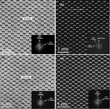
| Figures 4458a (a) and (c) show HAADF images of Si [110] taken in a Cs-corrected STEM system at 30 kV and 60 kV, respectively. Si (silicon) dumbbells, in which two Si columns are separated by 136 pm, are clearly shown in both cases. In Figure 4458a (b), the Fourier transform of the HAADF image (a) contains a clear -224 spot (corresponding to the lattice spacing of 111 pm), while in Figure 4458a (d), the Fourier transform of the HAADF image (c) shows clear -115 and -440 spots (corresponding to the lattice spacings of 105 and 96 pm, respectively).
Figure 4458a. (a) and (c) HAADF images of Si [110] taken at 30 kV and 60 kV, respectively, and (c) and (d) The Fourier transform of the HAADF image (a) and (b).
[2]
Figure 4458b shows the resolved Si (silicon) structures by UT-SA JEOL JEM-ARM 200F. Figure 4458b (b) demonstrates that HAADF image gave at least 78 picometer spatial resolution.
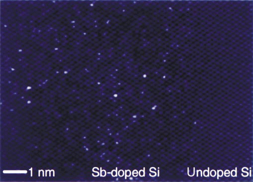
Figure 4458b. (a-b) Bright field (BF) and HAADF STEM images of Si [110] taken at 200 kV on JEOL JEM-ARM 200F. The HAADF image shows spatial resolution down to 0.078 nm, while the BF image resolves spatial information < 0.1 nm. (c-d) Bright field (BF) and HAADF STEM images of Si [110] taken at 120 kV on JEOL JEM-ARM 200F. Both the HAADF and BF images show spatial resolution down to < 0.1 nm. Voyles et al [1] analyzed Sb (antimony) doped Si (silicon) in the <110> zone-axis orientation using ADF-STEM (annular dark-field scanning transmission electron microscopy) operated at 200 kV, directly observed individual Sb atoms at atomic-resolution, and identified the Sb clusters in Si responsible for the saturation of charge carriers. The size, structure, and distribution of these clusters were determined with a Sb-atom detection efficiency of almost 100%. The brightest dots on the left in the ADF-STEM image in Figure 4458c are atomic columns containing at least one Sb atom and the undoped region on the right shows no such very bright dots. Regarding the quality of the TEM sample, their simulations showed that for a Si column containing a single Sb atom to be more than 25% brighter than a pure Si column, the sample must be less than 50 Å thick. Random variations in thickness must be less than the contrast of one Sb atom, and the surfaces must be free from native amorphous SiO2 layers and amorphized bulk Si layers.
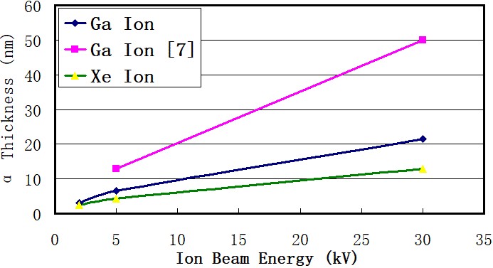
Figure 4458c. ADF-STEM image of a cross section of highly Sb-doped Si. It should be mentioned that no displacement damage in crystalline silicon is caused in TEM at imaging voltages of 100 kV or lower while displacement damage can be induced at 200 kV accelerating voltage or higher. [1] Figure 4458d shows the typical thickness of amorphous layer on each surface of silicon (Si) TEM samples experimentally prepared by FIB technique. Especially note that the thickness of the Si amorphous layer induced by 2 kV ions remains 3 nm even though this beam energy is very low in general. Furthermore, if the two surfaces of the TEM samples are prepared by FIB, the total thickness of the amorphous layers is doubled.
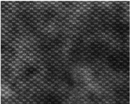
Figure 4458d. Typical thickness of the amorphous layer on each surface of silicon TEM samples experimentally prepared by FIB technique. Inada and Zhu, et al. [3] obtained high-resolution secondary electron microscopy (HRSEM) images of silicon (Si) TEM specimens along (110) direction, taken in a HD 2700C electron microscope using a 0.1 nm scanning probe with a Cs corrector. Figure 4458e shows the lattice fringes of a HRSEM image taken from a TEM specimen covered with a 3 nm amorphous layer induced by FIB specimen preparation. The speckle contrast is due to variation in thickness of the 3-nm amorphous layer. They also found visible lattice fringes in very low intensity for a specimen with an amorphous Si layer of 8 nm thick, while there was only a little atomic contrast in the (110) lattice for a specimen with an amorphous Si layer of 28 nm thick.
Figure 4458e. HRSEM image of a Si TEM specimen along (110) direction. Adapted from [3] Si is easily oxidized in air during mechanical polishing for EM analysis. In some critical analyses (e.g. Si surface plasmon analysis) in EELS, Si TEM specimens are normally dipped in HF solution (e.g. 10% HF solution) to remove the surface oxide. However, a thin layer of SiOx may still exist due to exposure to air before loading into the TEM.
[1] P. M. Voyles, D. A. Muller, J. L. Grazul, P. H. Citrin, and H.-J. L. Gossmann, Atomic-scale imaging of individual dopant atoms and clusters in highly n-type bulk Si, Nature, 416 (2002) 826.
|
![HAADF images of Si [110] taken at 30 kV and 60 kV](image1/2235b.jpg)