=================================================================================
The main inelastic scattering mechanisms are:
i) Phonon excitation (heat).
ii) Plasmon excitation (valence electrons).
iii) Single electron excitation (inner and outer shell scattering).
iv) Direct radiation losses (Bremsstrahlung radiation due to deceleration of the electron beam in the Coulomb field of an atom).
v) Excitation of conducting electrons leading to secondary electron emissions.
For many solids, especially metals, the bonding electrons can be considered as a free electron gas. Plasmons that are oscillations of the free electron are generated when an incident electron travels through the gas. The plasmon energies increase with electron density so that EEL spectra in the low loss range can be used to estimate free electron density.
The plasmon interaction does not give specific element identification, but plasmon spectra are routinely used to measure the thickness of TEM specimens because more plasmons are excited as the electron goes through a thicker specimen. The first part of the EEL spectrum (EELS) is related to basic excitation processes of high probability and is explained in terms of multiple scattering. These primary excitation processes include interband transitions, surface and bulk plasmons. Inelastic scattering from outer-shell electrons is visible as plasmon peak(s) in the EELS spectrum range of 2 – 50 eV. As shown in Figure 3997a, at higher energy loss, the electron intensity decreases rapidly.
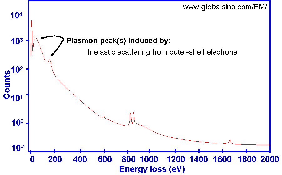
Figure 3997a. Plasmon peak(s) induced by inelastic scattering from outer-shell electrons.
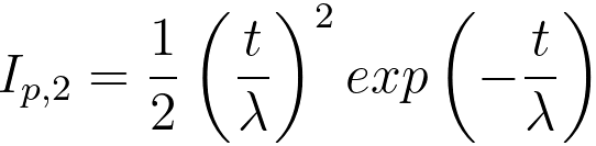
In thick specimens in TEM measurements, two or more plasmons can be excited by a single primary electron, inducing double and/or triple plasmon peaks in the EELS spectrum. In EELS the plasmons can have energy overlapping with signals due to the transitions of single electrons between the outermost bands of electron energies. The plasmon peaks are generally broad, with energies which are not uniquely representative of the specimen. There are not too many EELS applications based on plasmon peaks, but recently the plasmon mode is used for analysis of nanostructures. The intensity of plasmon signal can be given by,
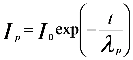 ----------------------------------- [3997a] ----------------------------------- [3997a]
where,
λ -- The mean free inelastic path of electrons for plasmon excitation,
t -- The specimen thickness,
I0 -- The intensity of the incident electron beam
.
The integrated area under the nth plasmon loss can be given by, [1]
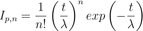 ------------------------- [3997b] ------------------------- [3997b]
The integrated area under the first plasmon loss can then be given by,
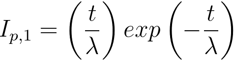 ------------------------- [3997c] ------------------------- [3997c]
The integrated area under the second plasmon loss can then be given by,
 ------------------------- [3997d] ------------------------- [3997d]
Based on Equations 3997b-d, Stephens [1] suggesed that the technique of energy
loss spectroscopy is only viable if the foil is less than about λ thickness.
Table 3997 shows that electrons interact with 1 electron, many electrons, 1 nucleus, and many nuclei in solids.
Table 3997. Effects of interactions of electrons in solids.
| |
Interaction with electron(s) |
Interaction with nucleus/nuclei |
| |
1 electron |
Many electrons |
1 nucleus |
Many nuclei |
| Scattering type |
Inelastic |
Inelastic |
Quasi-elastic |
Elastic |
Inelastic |
| Scattering effect |
Electron Compton effect; electron excitation (from 50 eV to a few keV: EDS and EELS) |
Plasmon excitation (< 50 eV, ~100 nm TEM specimen); Cerenkov effect |
Rutherford scattering; phonon scattering (< 1 eV, heat) |
Bragg scattering |
Bremsstrahlung |
Figure 3997b shows the schematic illustration of laterally resolved EELS across the multi-layers in the specimen. The horizontal stripes in Figure 3997b (a) represent the multi-layers in the TEM specimen. At high dispersion (a low eV/channel value), the curvatures of the zero loss (ZL) and plasma peaks on the CCD indicates the non-isochromaticity of the filter, while at low dispersion the curvature of the ZL is hardly visible.
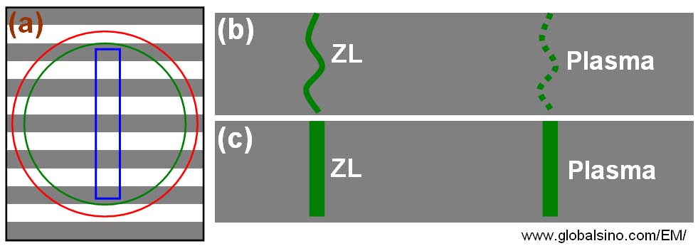
Figure 3997b. Schematic illustration of the laterally resolved EELS across the multi-layers in the specimen. (a) The slit aperture (in blue) across the interface of the multi-layers. The red (bigger) and green (smaller) circles represent the illumination area by the electron beam and the round spectrometer entrance aperture, respectively. (b) At high dispersion (a low eV/channel value), the curvatures of the zero loss (ZL) and plasma peaks on the CCD indicates the non-isochromaticity of the filter. (c) At low dispersion the curvatures of the ZL and plasma peaks is hardly visible.
[1] A. P. Stephens, Quantitative microanalysis by electron energy-loss spectroscopy: Two corrections, 5 (1–3) (1980), 343-349.
|