Chapter/Index: Introduction | A | B | C | D | E | F | G | H | I | J | K | L | M | N | O | P | Q | R | S | T | U | V | W | X | Y | Z | Appendix
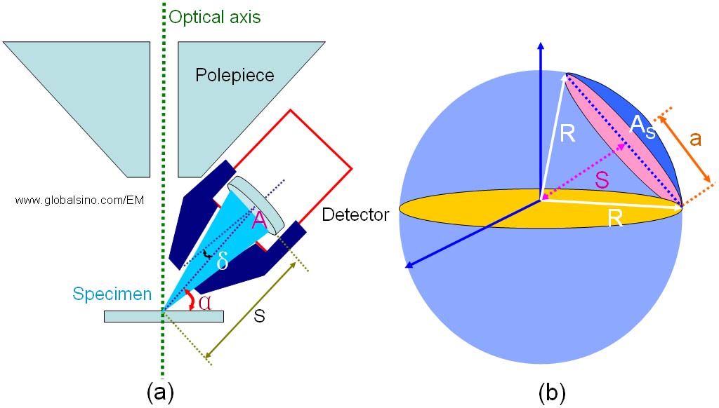
| For X-ray measurements, e.g. EDS, two main factors that affect the number of X-ray photons which reach the detector are: Other than the collection angle in EDS system, another important parameter is the take-off angle (α). As shown in Figure 4630a, the take-off angle is the angle between the specimen surface (at 0 ° tilt of specimen) and a line to the center of the detector (detector axis). In other words, it is defined by working distance and "bore axis" of the mounted EDS detector. This angle needs to be optimized so that the count rate of the detector is maximized.
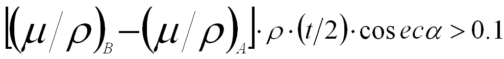
Figure 4630a. Schematic showing the positions of the EDS detector and specimen. In EDS measurements, the path of X-ray absorption mainly depends on two factors: High take-off angles decrease absorption of the X-rays, while low take-off angles increase absorption because the X-rays must penetrate more material. X-ray absorption increases rapidly for take-off angles under 25°, but is relatively constant for angles greater than 35°. Table 4630 lists the take-off angles and relative count rates of EDS systems on some microscopes. The count rates on ARL microprobes are ~30% higher than on MAC microprobes simply due to the higher take-off angle. In practice, the absorption correction is generally the most important. For any set of two elements A and B, the absorption correction will be needed if: For the same reason, the peak to background ratios (P/B) are better with higher take-off angles. For two adjacent elements in the periodic table, their (μ/ρ) values are similar so that the absorption does not severely affect the ratio of the intensities of their x-ray lines. Table 4630. The take-off angles and relative count rates of EDS systems on some microscopes.
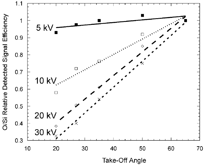
The effect on the analysis of SiO2 in terms of the measured O/Si ratio at different takeoff angles (20 to 65°) is plotted as a function of E0 in Figure 4630b. In the E0 range of 10 - 30 kV the effect is very large with the change of the takeoff angle because of the large change of X-ray absorption path, inducing significant change of absorption of low energy O X-rays. At low E0 of 5 kV, the interaction volume is small, so the change of X-ray absorption with the takeoff angle is limited; as a result, the takeoff angle has only a minor effect on the accuracy of analysis by measuring the O/Si ratio.
Figure 4630b. The O/Si ratio, obtained from SiO2, as a function of E0 [1]. However, in modern high-resolution TEM instruments, the detectors normally have a small take-off angle of 11 - 25°. Fortunately, it is possible to increase the total take-off angle to ~40° by tilting the specimen. However, the take-off angles are usually in the range of 30 - 45° for SEM. For the TEM configuration with a top-entry type EDS detector, the detector is placed above the objective lens in a TEM system with a high viewing angle (e.g. 70 °) to a horizontal specimen. Since X-rays entering the detector take a large take-off angle (TOA) against the specimen, a high accuracy of quantitative analysis can be obtained.
[1] Edward D. Boyes, Analytical potential of EDS at low voltages, Mikrochim. Acta 138, 225-234 (2002).
|
 ------- [4630]