
Chapter/Index: Introduction | A | B | C | D | E | F | G | H | I | J | K | L | M | N | O | P | Q | R | S | T | U | V | W | X | Y | Z | Appendix
| In EDS measurements, X-rays can be generated when an incident electron beam irradiates at the surface of materials. Characteristic or continuum X-rays with sufficient energy can induce the emission of an X-ray of lower energy if the X-ray generated in the specimen has sufficient energy to eject an electron in an inner shell of another atom. Therefore, some secondary X-rays (so-called x-ray fluorescence), however, can also be generated due to partial energy absorption of primary X-rays (generated by the electron beam). In this case, the characteristic X-rays from a heavier element photoionize atoms of lighter elements. This secondary X-ray generation occurs when the energy of a strong characteristic peak is above the ionization threshold of another element. For instance, the characteristic intensity of the lower energy X-ray of element A is overestimated due to its secondary X-ray fluorescence induced by the characteristic X-rays emitted by element B, resulting in overestimating the measured concentration of element A and underestimating that of element B. This happens in the EDS measurement of Cu-Fe alloy. The energy of Cu Kα radiation (8.04 keV) is sufficient to excite Fe K X-rays (7.11 keV). Therefore, the iron concentration would be overestimated due to the fluorescence by copper, while the Cu concentration would be underestimated due to the strong absorption by iron. The magnitude of the fluorescence corrections is generally ~1.5%, while the largest was a ~5% correction made to the Co-Cu sample. [2] The fluorescence correction in EDS measurements depends on: It was proposed that the primary X-ray generation occurs uniformly along the line of the electron beam in specimen in EMs [1] as shown in Figure 4648. The fluorescence enhancement of the lower energy X-ray of element A can be given by, where, As indicated in Equation 4648a, determination of the correction for X-ray fluorescence within the EM specimen requires the knowledge of the specimen thickness. Fortunately, there are some techniques which can be used to measure the specimen thickness. IFA/IA (= XA) is normally called enhancement factor for the element A. Therefore, for a specimen in which the element B causes fluorescence of element A, the experimental composition need to be corrected by, In practice, the phenomenon of secondary fluorescence is rarely a problem, especially in silicates, because its efficiencies are low for the elements of Z < 20 and tend to be negligible. In accurate EDS quantifications, the appropriate corrections such as stopping power, back-scattering, X-ray absorption and secondary X-ray fluorescence within the specimen, should be evaluated and applied to the raw EDS data. Note that the effects of absorption are nearly always much more serious than characteristic fluorescence for specimens of similar thicknesses. TEM specimens can be used to simplify EDS measurements, especially quantifications, as the thin specimens avoid significant x-ray absorption and secondary x-ray fluorescence events. Those two factors typically cause significant EDS inaccuracy with bulk specimens in an electron beam microprobe or a scanning electron microscope.
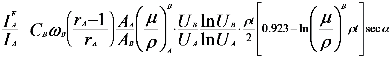
[1] Nockolds, C., Nasir, M. J. and Lorimer, G. W. (1979) In
Electron Microscopy and Analysis (T. Mulvey, ed.)
I.O.P., London, 417.
|
 ------ [4648a]
 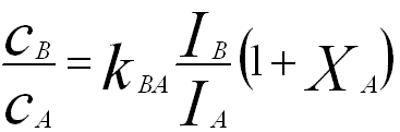 ------------------- [4648b]