Absorption of Outgoing X-Ray in EDS Analysis - Practical Electron Microscopy and Database - - An Online Book - |
|||||||||||||||||||||||||||||||||||||||||||||||||||||||||||||||||||||||||||||||||||||||||||||||||||||||||||||||||||||||||||||||
| Microanalysis | EM Book https://www.globalsino.com/EM/ | |||||||||||||||||||||||||||||||||||||||||||||||||||||||||||||||||||||||||||||||||||||||||||||||||||||||||||||||||||||||||||||||
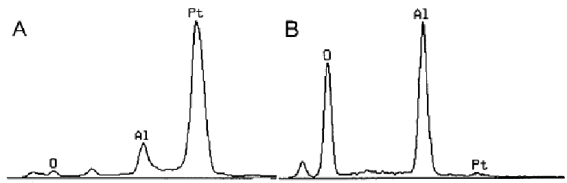
In EDS measurements, X-rays can be generated when an incident electron beam irradiates at the surface of materials. X-ray, however, can also be absorbed by the materials themselves (especially for thick TEM samples and bulk SEM samples) during the EDS data acquisition process. This process is called self-absorption of outgoing X-ray. This process can be minimized if a thin film is used, e.g. thin samples in TEM measurement. However, for thick samples in TEM/STEM measurements and bulk samples in SEM measurement, due to this absorption effect, the measured X-ray intensities are a function of the escape depth and of the absorption characteristics of the sample. In fact, for SEM-EDS measurements on bulk materials, the absorption of X-rays is also increased with higher accelerating voltage. Especially, for the samples with higher Z and the X-rays at lower energies, this correction becomes even more important. Note that the abrupt appearance of an absorption edge in the continuum of the spectrum represents a severe deviation from linearity even though these abrupt steps are smooth in appearance due to the low energy resolution of the X-ray detector. When the X-ray absorption is significant, especially for SEM-EDS measurements on bulk samples, the shape of the depth distribution of X-ray production is crucial, and thus ZAF and Phi–Rho–Z models should be used. However, the mass absorption coefficients are still problematic because significant uncertainties exist even in absorption-corrected ZAF and Phi–Rho–Z models. X-ray absorption is a function of the energy of X-rays. Low energy peaks will be more strongly absorbed than high energies ones. Figure 4650a shows EDS analysis of materials consisting of Al, Pt, and O elements. At high accelerating voltage (30 keV), the spectrum shows a dominant Pt M (~2.1 keV) peak. The O K (~0.5 keV) peak is very weak due to the matrix absorption. That is, low energy O K (~0.5 keV) X-rays are absorbed more significantly than high energy Pt M X-rays, and thus the X-ray escape range is reduced sufficiently for the O K X-ray. As the accelerating voltage is reduced to middle voltage, and then to low voltage (4 keV), the absorption of O K X-rays becomes less significantly because of its shallow interaction volume.
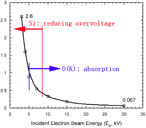
Figure 4650b shows the ratio of O and Si X-rays signals, taken from quartz (SiO2), as a function of incident electron beam energy (E0), detected with a Si(Li) ATW detector. The plot extends from a very low O/Si ratio (0.067) at 30 kV through an analysis at 5 kV which closely reflects the correct chemistry of the sample to analyses at low voltages of < 5 kV with O/Si >> 1. The final data point is 2.6 at 2.7 kV. Above 5 kV the accuracy of the analyses are limited primarily by differential absorption of the O(K) X-ray signal. At low voltage the under representation of Si reflects the reduction in the fluorescent yield with reducing overvoltage (U).
In accurate EDS quantifications, the appropriate corrections such as stopping power, back-scattering, X-ray absorption and secondary X-ray fluorescence within the sample, should be evaluated and applied to the raw EDS data. Note that the absorptions of x-rays can also affect the calibration of x-ray signals and the effects of absorption are nearly always much more serious than characteristic fluorescence for samples of similar thicknesses. For instance, Si and Fe are often used as standards, however, the absorptions of their x-rays are not equal. The error of the detected Si x-ray intensity, due to Si Kα absorption in the sample, is larger than that of Fe Kα. Furthermore, determination of the correction for X-ray absorption within the sample requires the knowledge of the sample thickness. There are some techniques which can be used to measure the sample thickness. For thick TEM samples, k-factor correction due to X-ray absorption is needed in order to accurately quantify EDS measurements. Table 4650a lists examples of thicknesses at which the thin-film approximation is no longer valid due to X-ray absorption effects in specific materials.
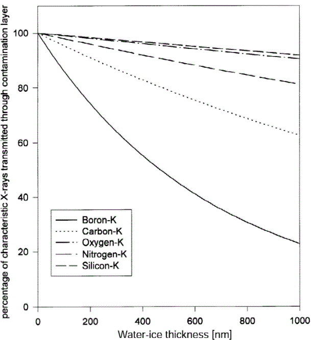
The measured X-ray intensity, after removing the losses of X-rays through the absorption process, can be given by, Figure 4650c shows the percentage of x-ray transmitted through an H2O-ice contamination layer depending on the thickness of the H2O-ice layer up to 1 μm. As expected, the absorption effect of ice layer is greatest for the low-energy boron x-rays and the least for the silicon signal. Such H2O-ice layer is normally formed in cryo-TEM measurements.
It is necessary to mention that the x-ray absorption is also dependent on the probe size. Wood et al. [2] suggested that the x-ray absorption in the sample is not significant (<5%) when the probe size is larger than ~9 nm, while it shows significant absorption if the electron probe is smaller, e.g. in the range of 5-10 nm in diameter. Table 4650b lists some examples of absorption percentage out of generated x-ray. It can be seen that the critical thicknesses of Ni-8 mol% Al and Ni-50 mol% Al used in this study are 25 and 49 nm for 5% absorption, respectively.
[1] Edward D. Boyes, Analytical potential of EDS at low voltages, Mikrochim. Acta 138, 225-234 (2002).
|
|
||||||||||||||||||||||||||||||||||||||||||||||||||||||||||||||||||||||||||||||||||||||||||||||||||||||||||||||||||||||||||||||