Chapter/Index: Introduction | A | B | C | D | E | F | G | H | I | J | K | L | M | N | O | P | Q | R | S | T | U | V | W | X | Y | Z | Appendix
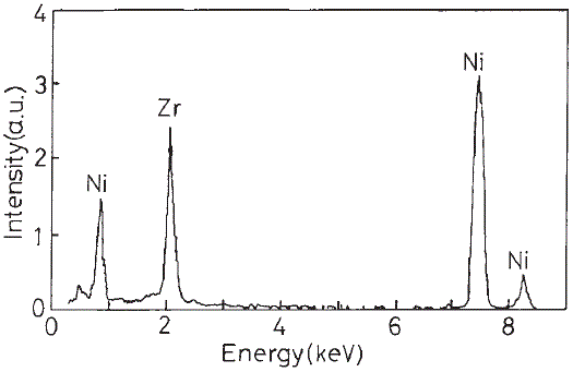
| Figure 1825 shows EDS profile of a Zr-Ni thin film.
Figure 1825. EDS profile of a Zr-Ni thin film. [1] Note that, in practice, Ni X-rays are also generated from SEM/TEM specimen chamber, column and apertures by Rutherford backscattered electrons because these parts of the SEM/TEM systems contain such element. These spurious X-rays can often be detected by the EDS detector. EDS-TEM specimen holders and stray aperture are normally used to reduce such spurious X-rays. As discussed on page4650, X-ray absorption is a function of the energy of X-rays. Low energy peaks will be more strongly absorbed than high energies ones. For thick TEM samples, k-factor correction due to X-ray absorption is needed in order to accurately quantify EDS measurements. Table 1825 lists Ni-examples of thicknesses at which the thin-film approximation is no longer valid due to X-ray absorption effects in specific materials.
[1] Masahiro Kitada and Fumiyoshi Kirino, Effects of Sputter Order and Oxide Layer on Amorphous Formation of Zr-Ni Thin Film System, Materials Transactions, Vol. 46, No. 2 (2005) pp. 277 to 280.
|
||||||||||||||||||