| |
For correct detection and analysis of EDS profiles and maps, the users need to be aware of some artifacts such as escape peaks, sum peaks, peak overlaps, incomplete charge collection, and excessive deadtime. Modern analytical software used in EDS measurements can generally take some artifacts into account, but no software is perfect. On the other hand, many users look at the raw spectra, while the software may not have labeled whether there are artifacts or which ones are.
Spurious X-rays can be generated in the region of interest (ROI) or other areas in the specimen, but do reach the detector and can be confused with X-rays from the specimen, causing serious problems. There are many sources of spurious x-rays, including:
i) Spurious x-rays, e.g. see page4479, can be generated in the specimen itself, for instance, by the following effects:
i.a) The backscattered electrons of the high-energy incident beam are induced by the specimen, and then by bulk material such as the objective pole-pieces. These backscattered electrons can then generate continuous and characteristic X-rays from the specimen, its support grid, and the specimen holder. The spurious X-rays generated from SEM/TEM specimen chamber, column and apertures by Rutherford backscattered electrons are normally Cu, Fe, Ni, and Cr X-rays because these parts of the SEM/TEM systems contain such elements. Tilting the specimen may eliminate such peaks generated from the specimen as the distribution of the backscattered electrons will change.
i.b) The continuum X-rays produced at the region being analyzed in the specimen will fluoresce in the specimen region, the support grid, etc.
ii) Spurious x-rays can be generated from stray radiations. For instance, hard x-rays can first be generated in the illumination system of the microscope
from electron interactions with the column components and then transmitted through the condenser aperture. These X-rays induce fluorescence in the specimen grid and elsewhere in the area around the specimen.
iii) Due to un-collimated electrons and those scattered from the bore of the C2 aperture can excite X-rays. In this case, spurious x-rays can rise from the signals from other surrounding materials (e.g. from the solid angles of Ω3 and Ω4, involving a large volume of the stage and its environment) as shown in Figure 4638.
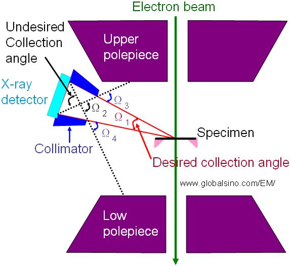
Figure 4638. Schematic illustration of the desired collection angle in an EDS detector system.
iv)
Spurious X-rays can be generated from specimen coatings, e.g. Au is commonly used to avoid charging effect in SEM measurements. If the Au X-rays are a problem, then another coating material should be used.
It is necessary to highlight that except for the random errors from counting statistics, some factors, however, will contribute systematic errors. Those factors are mainly:
i) The accuracy of the chemical composition of the standard (if calibration or correction of kAB factors is applied).
ii) The presence of spurious X-rays.
iii) The inaccuracy of evaluation of the specimen thickness.
iv) The deconvolution of overlapping peaks.
v) Thee background-fitting routine.
Fortunately, in modern TEM systems, such spurious X-rays can be minimized by the following methods:
i) Employ shielding and better designs of specimen stages and X-ray detectors. Manufacturers of TEM instruments and EDS detectors are well aware of this issue, and have been doing the best in designs to minimize spurious X-rays.
ii) Remove the objective aperture during analysis. The objective aperture (e.g. in TEM) not only generates hard X-rays and potentially damages the EDS detector, but also causes unwanted X-ray peaks in the obtained spectrum.
iii) Employ an extra-thick, 'top hat' C2 aperture.
iv) Use an stray aperture in the column above the specimen. The stray aperture protects the specimen from the impingement of X-rays because it can strongly absorb the signals from stray radiation and thus, improves the accuracy of the measurements.
v) Use materials with low atomic numbers for the specimen holder and support grid.
For instance, if small particles are analyzed with EDS, Be or polymeric grids with carbon films can be used instead of metal grids since Cu grids produce Cu peaks in the X-ray spectra. Those materials with low atomic numbers do not produce significant spurious X-ray signals.
Furthermore, X-ray artifacts can also rise from diffraction effects.
To further avoid artifacts in EDS measurements, more considerations must be taken into account, especially when you are investigating unexpected elements. You should have a suitable sample thickness because the sample gives too weak signal if the sample is too thin and cause strong X-ray absorption if the sample is too thick. For instance, the quantitative analysis will not be accurate if a line scan was done across different grains at different crystalline orientations.
Except for the method of "hole count" in X-ray measurements, spectral artifacts can further be determined by a close inspection of spectra from various pure-element and compound standards at multiple accelerating voltages in EMs.
|
|