Chapter/Index: Introduction | A | B | C | D | E | F | G | H | I | J | K | L | M | N | O | P | Q | R | S | T | U | V | W | X | Y | Z | Appendix
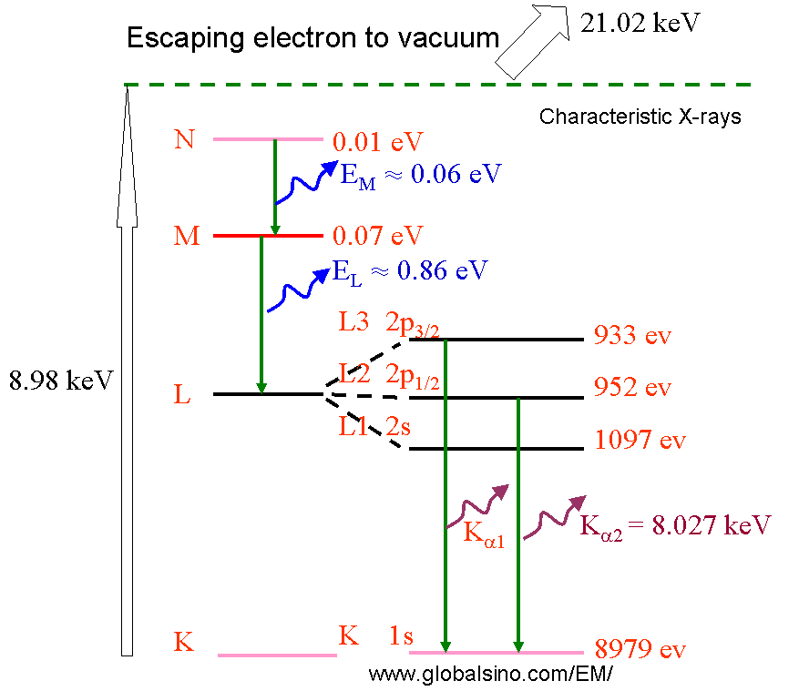
| The values of characteristic X-ray energies of copper (Cu) can be obtained, e.g. for Cu K, by subtracting the energy of the L shell (binding) energy from that of the K shell (binding) energy as shown in Figure 4479a.
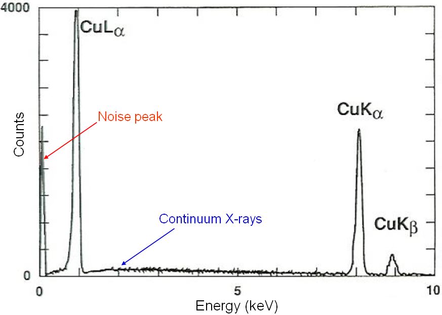
Figure 4479a. Extraction of values of characteristic X-ray energies of Cu. As examples, according to Figure 4479a, we can calculate, Figure 4479b shows a typical EDS profile of pure copper. The natural peak widths are much narrower than the measured ones in the figure. A noise peak is also shown at very low energies.
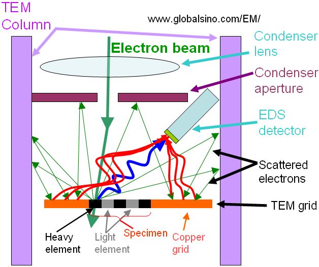
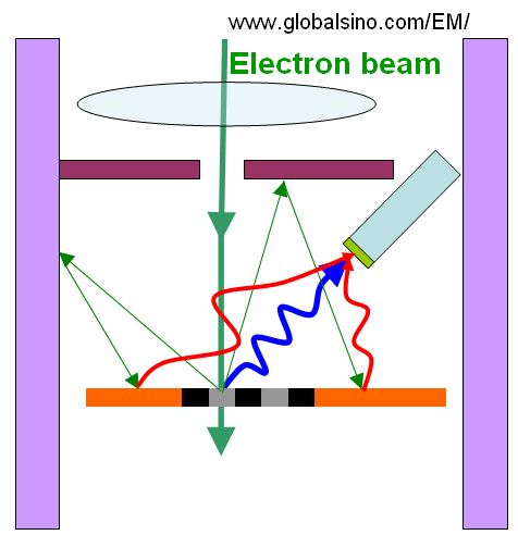
Cu grids are widely used as supporting grids in FIB (focused ion beam) prepared TEM specimens. However, artificial Cu signals can be induced due to the Cu grid itself, especially when Cu interconnect structures are analyzed in semiconductor industry. The origin of the artificial Cu signal is mainly electron scattering induced by the analyzing materials (see Figure 4479c). Therefore, the artificial Cu signal is higher when heavier elements, e.g. W and Pt, are measured because of their stronger scattering. On the other hand, the stray radiations originated from the analyzing heavy elements can also enhance artificial Cu signal. Other grids, such as nickel (Ni) and molybdenum (Mo) grids, can be used to avoid the artificial Cu signal but those grids induce their own artificial EDS signals. For this reason, depending on the interest, proper grids are usually selected for FIB-TEM specimen preparation. On the other hand, in practice, Cu X-rays are also generated from SEM/TEM specimen chamber, column and apertures by Rutherford backscattered electrons because these parts of the SEM/TEM systems contain such element. These spurious X-rays can often be detected by the EDS detector. EDS-TEM specimen holders and stray aperture are normally used to reduce such spurious X-rays.
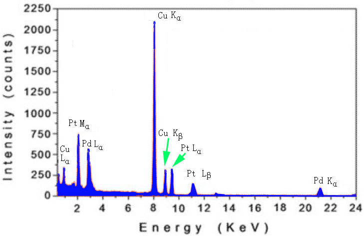
The EDS spectrum in Figure 4479d was taken from a nanoparticle (with Pt and Pd compositions of 50 at.% : 50 at.%) on holey carbon (C) film supported by a copper TEM grid. The copper signal in the spectrum was from the Cu grid (see page4638).
As discussed on page4650, X-ray absorption is a function of the energy of X-rays. Low energy peaks will be more strongly absorbed than high energies ones. For thick TEM samples, k-factor correction due to X-ray absorption is needed in order to accurately quantify EDS measurements. Table 4479 lists Cu-examples of thicknesses at which the thin-film approximation is no longer valid due to X-ray absorption effects in specific materials.
|
|||||||||||||||||||||||||||