=================================================================================
Similar to SEM, FIB (focused ion beam) detects the secondary electrons produced at each raster position of a focused beam on the sample. The magnifications can be up to ~100 000 times with a very good depth of field. The operation of a FIB starts with a liquid metal ion source (LMIS) as shown in Figure 4511a. FIB normally uses a primary beam of Ga ions as a milling and imaging probe. By adjusting the strength of the electrostatic lenses and the effective aperture sizes, the probe current density is altered from tens of pA to several nA and the corresponding beam diameter is from ~5 nm to ~0.5 µm. Table 4511 lists the function of each part in the FIB.
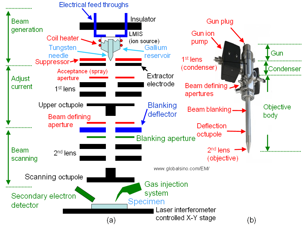
Figure 4511a. Schematic illustration of the LMIS and lens system of an FIB.
Figure 4511b shows the first Rossendorf FIB system created in 1987. This FIB had a 40-keV LMIS-Ga ion beam at a spot size of 500 nm.
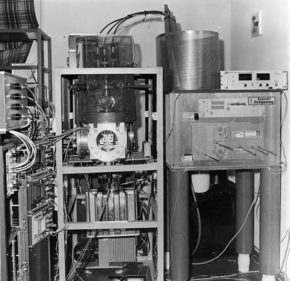
Figure 4511b. The first Rossendorf FIB system. [14]
Table 4511. The parts and their functions in FIB systems.
Part |
Function |
|
Provide positively charged ions |
Ion Column |
|
Improves the distribution of extracted
ions |
|
High tension used for ion extraction: Typical accelerating voltage in FIB systems ranges from 1 to 30 keV |
|
First refinement |
1 st lens (condenser lens) |
Parallelize the ion beam: probe forming |
|
Stigmator |
|
Defines current: A set of apertures define the probe size and provides a range of ion currents (10 pA – 30 nA) |
|
Beam blanking: Beam blankers are used to deflect the beam away from the centre of the column |
Blanking aperture |
Beam blanking |
Lower octopole |
Raster scanning |
2nd lens (objective lens) |
Beam focusing |
Stage |
Support and operate samples |
Gas Delivery |
|
Detector |
Imaging |
Computer |
Provide integrated image processing |
Vacuum System
|
Provide vacuum |
Low energy FIB systems (typically, 5 - 50 kV) have various applications:
i) Local removal of materials by physical sputtering.
i.a) Cross section. Ideal requirement: flat cut.
i.b) TEM lamella. Ideal requirement: thin & defect free.
ii) Milling/etching with or without use of gases, similar to laser beam direct
writing (LBW).
ii.a) Pillar. Ideal requirement: steep sidewalls, no overetch for mechanical testing.
ii.b) Nanostructuring. Ideal requirement: no redeposition, smooth surfaces.
iii) Preferential removal of specific materials.
iv) Local deposition of materials by ion induced chemistry.
v) Grain imaging.
vi) Modification of integrated circuits (ICs). [8]
vii) Preparation of TEM specimens. [9]
viii) Interfacial microstructure characterization.
ix) Failure analysis of ICs by local cross sectioning and imaging. [10]
x) Secondary electron surface inspection.
xi) Micro-electro-mechanical
systems (MEMS) development. [11]
xii) Fabrication of functional scanning probes. [12, 13]
xiii) Lithography, similar to electron beam lithography (EBL).
The most important advantage of FIBs in all these applications is the maskless generation of an ion intensity pattern on the surface of the target. Therefore, FIB technique has been applied as a general fabrication, characterization, and specimen preparation tool for both material and biological sciences. In most (but not all) cases the desired function of the ion beam in FIB is material removal due to sputtering.
Especially, FIB systems have been widely used for TEM specimen preparations, which allows site-specific preparation with high throughput and precise localization of the defective spots and small lines, for instance, in semiconductors. FIB technique has become common in materials science laboratories and is also used to produce channeling contrast images and to prepare samples for scanning electron microscopy (SEM) and transmission electron microscopy (TEM). However, the artifacts of the FIB preparation process, including curtaining and beam-induced damage, degrade the specimen quality, and thus affect the quality of the TEM imaging.
Since a monovacancy was first observed by TEM in low-dimensional carbon structures [1], the studies of point defects in monolayered materials using TEM have been attracting scientists' interest. For instance, the vacancies and topological defects in grapheme, edge structures and point defects in single layer hexagonal boron nitride (h-BN) [2, 7], monovacancies in WS2 nanoribbons [3] have been successfully identified at atomic level [4–6]. Unfortunately, this type of analyses was only achieved in “natively” grown nanomaterials but no applications have been performed successfully in samples prepared from bulk materials, e.g. by FIB (focused ion beam), mainly because of preparation-induced damages.
[1] Ayako Hashimoto, Kazu Suenaga, Alexandre Gloter, Koki Urita, & Sumio Iijima,
Nature (London) 430, 870 (2004).
[2]
O. Krivanek et al., Nature (London) 464, 571 (2010).
[3] Z. Liu et al., Nature Commun., 2, 213 (2011).
[4] K. Suenaga et al., Nature Nanotech. 2, 358 (2007).
[5] J. Meyer et al., Nano Lett. 8, 3582 (2008).
[6] C. O. Girit et al., Science 323, 1705 (2009).
[7] Kazu Suenaga, Haruka Kobayashi, and Masanori Koshino, Core-Level Spectroscopy of Point Defects in Single Layer h-BN, Physical Review Letters, 108, 075501 (2012).
[8] L.R. Harriot, A. Wagner, F. Fritz, “Integrated circuit
repair using focused ion beam milling”, J. Vac. Sci.
Technol. B, vol. 4, pp. 181, 1986.
[9] A. Yamaguchi, T. Nishikawa, “Low-damage specimen
preparation technique for transmission electron
microscopy using iodine gas-assisted focused ion beam
milling”, J. Vac. Sci. Technol. B, vol. 13(3), pp. 962,
1995.
[10] E. C. G. Kirk, R. A. Mc Mahon, J. R. Cleaver, and H. Ahmed. Scanning ion microscopy and microsectioning of electron
beam recrystallized silicon on insulator devices. J. Vac. Sci. Technol., B 6:1940–1943, 1988.
[11] J. H. Daniel, D. F. Moore, and J. F. Walker. Focused ion beams for microfabrication. Eng. Sci. Educ. J., 7(2):53–56,
1998.
[12] A. Olbrich, B. Ebersberger, C. Boit, P. Niedermann, W. H¨anni, J. Vancea, and H. Hoffmann. High aspect ratio all
diamond tips formed by focused ion beam for conducting atomic force microscopy. J. Vac. Sci. Technol., B 17:1570–1574,
1999.
[13] A. Kueng, C. Kranz, A. Lugstein, E. Bertagnolli, and B. Mizaikoff. Integrated AFM-SECM in tapping mode: Simultaneous
topographical and electrochemical imaging of enzyme activity. Angew. Chem. Int. Ed., 42:3238–3240, 2003.
[14] L. Bischoff, T. Chudoba and F.K. Naehring, Physical Research 13 (1990) 42.
|