Chapter/Index: Introduction | A | B | C | D | E | F | G | H | I | J | K | L | M | N | O | P | Q | R | S | T | U | V | W | X | Y | Z | Appendix
| Table 2402a. Main edges of Hf used in EELS analysis.
In order to record the signals of Hf together with other elements in a single EEL spectrum, a proper edge of Hf should be selected. For instance, Table 2402b lists some application examples of Hf edges used in the particular cases.
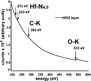
Figure 2402a shows an EELS experimental spectrum recorded from an HfO2 material. It is clear that the two Hf edges (N4,5) are very weak.
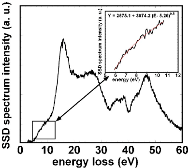
Figure 2402a. EELS experimental spectrum recorded from an HfO2 material. Adapted from [1] Band gap can be determined based on Bethe’s theory. In this case, the SSD (single scattering distribution) spectrum is described to be proportional to the product of the joint density of states (JDOS). Here, the JDOS is given by, Therefore, Eg can be extracted by fitting the single scattering spectrum using Equations [2402a] and [2402b]. Figure 2402b shows the band gap determination of the HfO2 layer in a Si/SiO2/HfO2/poly-Ge stack by using Equation 2402a (direct band gap [Eg = 5.26 eV] for HfO2).
Figure 2402b. Band gap determination of the HfO2 layer in a Si/SiO2/HfO2/poly-Ge stack. Adapted from [1]
[1] Marie C. Cheynet, Simone Pokrant, Frans D. Tichelaar, and Jean-Luc Rouvière, Crystal structure and band gap determination of HfO2 thin films, Journal of Applied Physics 101, 054101 (2007).
|
 for a direct band gap, ------------- [2402a]
  for an indirect band gap ------------- [2402b]