Chapter/Index: Introduction | A | B | C | D | E | F | G | H | I | J | K | L | M | N | O | P | Q | R | S | T | U | V | W | X | Y | Z | Appendix
| In IC devices, fluorine corrosion can be induced by F contamination as some F-based chemical gases and materials such as CF4, CHF3, SF6, HF, BOE (NH4F + HF) etc are used in microelectronics wafer fab. On the other hand, wafer shipment
package foam materials may also cause the F contamination and corrosion. Table 2436a. Fluorine contamination in IC devices.
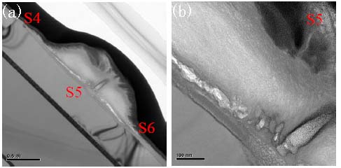
Figure 2436a shows an example of C, O, and Si contaminated bond pads. Area S6 had an abnormal film on the native Al oxide, while area S5 presented nonhomogeneous, loose and empty SixAlyCzOm materials in the hemispherical defect. These pad defects existed only at wafer edge because backside grinding was the root cause of the contamination.
Figure 2436a. Contaminated bond pads. Adapted from [2]
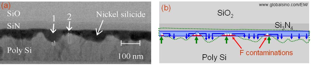
The TEM image in Figure 2436b (a) shows that the high resistance, undulate nickel silicide film that was essentially caused by fluoride contamination. This contamination originated from a chemical dry-cleaning process for silicon (Si) substrate prior to Ni sputtering. The undulate film consisted of thicker NiSi areas (e.g. arrowed by 1) and thinner NiSi2 areas (e.g. arrowed by 2). In Figure 2436b (b), the formation process of the Ni silicide film in different phases was:
Figure 2436b. Undulate NiSi + NiSi2 film formed due to fluoride contamination: (a) TEM image of nickel silicide film (Adapted from [5]). White arrow "1" points to thicker NiSi, while arrow "2" points to thinner NiSi2. (b) Schematic illustration of the formation process of the structure in (a). The blue box represents the area of the as-deposited Ni film. The area marked by the dotted green curve represents the final nickel silicide as shown in (a). The white spots indicate vacancies that are formed due to Ni out-diffusion during the initial annealing process, while the blue arrows indicate the direction of the Ni out-diffusion. The red lines at the initial interface between the as-deposited Ni and Si substrate represent fluoride (F) contaminants. The green arrows indicate the Si diffusion into the vacancy areas during the second annealing process. Note that the fluorine contamination on Si wafers can be investigated with XPS analysis.
[1] Y. N. Hua, S. Redkar, C. K. Lau, “A Study on Non-
Stick Aluminium Bondpads due to Fluorine
Contamination using SEM, EDX, TEM, IC, Auger, XPS
and TOF-SIMS Techniques,” Proceedings from the 28th
International Symposium for Testing and Failure
Analysis, Phoenix, Arizona, November, 2002, pp. 495-504.
|