=================================================================================
The measurement procedure of convergence semi-angle (α) is not difficult; however, the accuracy of the measurement strongly relies on the accuracy of the measurement of CBED pattern in the diffraction plane of the STEM or CBED.
The procedure of α determination is:
i) Prepare a crystalline TEM/STEM specimen with a known orientation.
ii) Measure the spacing (b) between Bragg discs as shown in Figure 2746a. Note that b is the distance between the centers of the 000 and 200 Bragg discs and is independent on the size of the selected aperture, but is determined by the Bragg angle and the camera length.
iii) Measure the diameter (a) of the image of condenser-aperture 2.
iv) Look for the values of Bragg angle (θb) for a particular reflection (for a given wavelength) from an existing database (e.g. bcc, hcp, and fcc). Note, b represents 2θb rather than θb.
v) The convergence semi-angle (α) of the probe is proportional to the ratio of the disc width (diameter of the image of condenser-aperture 2) to the disc spacing (a/b), and α can be calculated by,
 -------------------------- [2746] -------------------------- [2746]
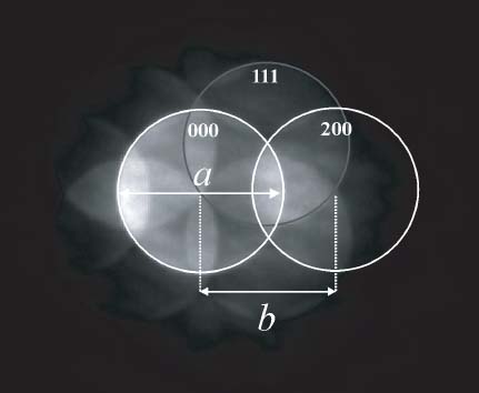
| Figure 2746a. Diffraction pattern of Si (silicon), oriented onto to 110 axis. Adapted from [1] |
For instance, it is very common that you use a {110} silicon crystalline TEM specimen to measure the convergence semi-angles, then you can follow the procedure below:
i) Record the accelerating voltage of your TEM system for the calculation of convergence semi-angles since the diffraction angles depends on the voltage. Here, we use 200 kV microscope as an example.
ii) Load the specimen with a double tilt TEM holder,
iii) Align the electron microscopy on the specimen in STEM mode by following all the procedures which you used for routine STEM imaging,
iv) Switch the microscope to Ronchigram mode,
v) Align Ronchigram to the center of the screen,
vi) Select and insert the condenser aperture which you want to measure the convergence semi-angle for,
vii) Align the condenser aperture to the center of the screen,
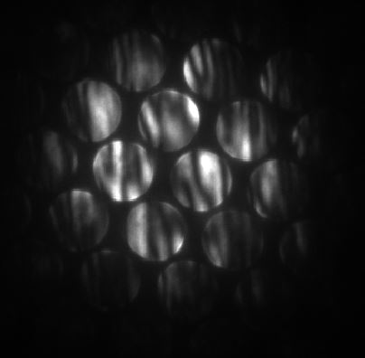
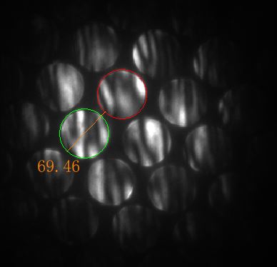
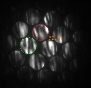
viii) Tilt the specimen to the [110] zone axis and record an image as shown in Figure 2746b (a),
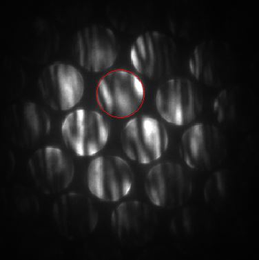
ix) Label the transmission beam as shown in the red circle in Figure 2746b (b),
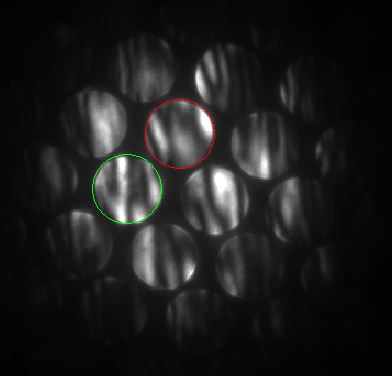
x) Identify and label a diffracted (111) beam as shown in the green circle in Figure 2746b (c),
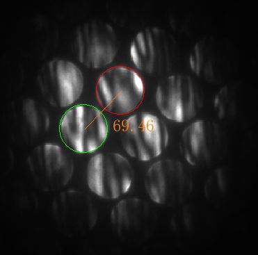
xi) Measure the distance (shown by the orange line in Figure 2746b (d)) between the centers of the red and green circles along their common diameter of the two circles as shown in Figure 2746b (d), or alternatively measure the distance between the two edges of the red and green circles along their common diameter of the two circles as shown in Figure 2746b (e). The numbers of the two measures are the same, of course. The units of the measures here is in pixel, and thus the measures are 69.46 pixels.
xii) Measure the diameter of any circle. Here, the diameter of the transmission beam is measured as 59.81 pixels. Of course, the diameters of all the circles are equal and are determined by the condenser aperture.
xiii) Find the reflection angle of (111) beam from page4489, which is 8.01 mrad for 200 kV.
xiv) Calculate the convergence semi-angle by using Equation 2746. Here, the semi-angle = (8.01*59.81)/(69.46*2) ≈ 3.45 mrad.
Figure 2746b. Example of measuring convergence semi-angles with a {110} silicon crystalline TEM specimen: (a) [110] zone axis of a Si crystal, (b) Transmission beam in the red circle, (c) Diffracted (111) beam in the green circle, (d) Distance between the centers of the red and green circles along their common diameter of the two circles, (e) Distance (69.46 pixels) between the two edges of the red and green circles along their common diameter of the two circles, and (f) Diameter of the transmission beam (59.81 pixels).
|
[1] M. Weyland and D. A. Muller, Tuning the convergence angle for optimum STEM performance, FEI nanoSolutions, (2006) 24.
|