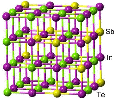
| In general, crystalline GST (GexSbyTez) thin films show two types of structures: [5, 61]
i) Metastable NaCl-cubic structure (space group Fm-3m).
In this structure, the 4A sites are occupied by Te atoms and the 4B sites are randomly occupied by Ge atoms, Sb atoms and 10-20% vacancies depending on the GST composition [5]. On the other hand, there is a relatively large displacement of Ge-atoms.
ii) Stable hexagonal structure (space group p-3m1).
Note that, in formation of GST crystals, a stacking disorder parallel to the basal plane increases with increasing cooling rates.
In poly-crystalline GST, excess Ge atoms and Sb atoms do not fill up the vacancies, but rather segregate on the grain boundaries.
In amorphous binary GeTe and quasibinary GST, the Ge-Te bonds are shorter and stronger than those in the corresponding crystals, and thus the amorphous phase is locally more ordered than the crystalline phase [62].
Table 3161. Structural properties of some GexSbyTez (GST) compositions.
|
XRD |
Electron diffraction |
HRTEM image |
Crystal structure |
Electrical resistivity |
Lattice constant
(nm) |
Atomic density (atom·Å-3) |
Crystall-ization tempera-ture (°C) |
Melting point (°C) |
Note |
Reference |
Amorphous Sb |
|
|
|
|
|
|
0.0321 |
|
|
|
[13] |
Crystalline Sb |
|
|
|
|
|
a = 0.43; c = 1.12 |
|
|
|
Space group R-3m. Interatomic distances: 0.296 nm and 0.430 nm. |
[13] |
|
|
|
|
|
|
|
|
|
|
Crystalline growth velocity 5.99 m/s. |
[15] |
AgInSbTe |
|
|
|
|
|
|
|
200 |
537 |
|
|
Amorphous Ag4In3Sb67Te26 |
|
|
|
|
|
|
0.0309 |
|
|
|
[20] |
Crystalline In3Sb67Te26 |
|
|
|
|
|
|
0.0324 |
|
|
|
[20] |
GaSb |
|
|
|
|
|
|
|
195 |
589 |
|
|
GeCu2Te3 |
|
|
|
|
|
|
|
250 |
500 |
|
[24] |
|
|
|
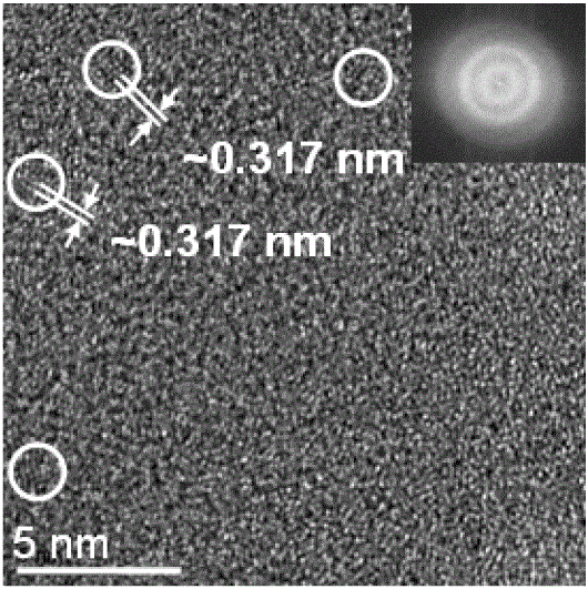
Medium-range ordering with fringe spacing of 0.317 nm:
 |
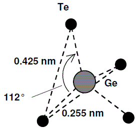
Asymmetrical tetrahedral structure:
 |
|
|
0.0334 |
182 |
725 |
Bond length: Ge-Te = 0.255±0.004 nm; Te-Te = 0.425±0.004 nm. Bond angle: Te-Ge-Te = 112°. Still various structure models for the local order. |
[16, 59] |
Amorphous 4%C- GeTe |
|
|
|
|
|
|
|
290 |
|
Improved amorphous phase stability compared to GeTe |
[63] |
Amorphous 10%C- GeTe |
|
|
|
|
|
|
|
340 |
|
|
[63] |
Crystalline GeTe |
|
|
|
|
|
|
|
|
|
Bond length: Ge-Te = 0.290±0.004 nm; Te-Te = 0.428±0.004 nm. Bond angle: Te-Ge-Te = 93°. |
|
GeTe |
|
|
|
|
|
Rhombohedral; a = 0.5996; α = 88.18° |
~0.0358 |
|
|
<400 °C has a trigonal (R-3m) structure (distorted NaCl type structure) |
[1, 2, 17] |
GeTe |
|
|
|
|
|
a = 0.60; α = 90° |
~0.0358 |
|
|
>400 °C has NaCl (B1) type structure |
[1, 2, 17] |
GeTe |
|
|
|
|
|
a' = 0.417; c' = 1.071 |
~0.0358 |
|
|
With an a, b, c stacking
sequence of close packed planes along the c'-axis of Te–Ge–Te–Ge–Te–Ge– |
[17] |
Amorphous Ge8Sb2Te11 |
|
|
|
|
|
|
0.0309 |
|
|
|
[17] |
Amorphous Sb2Te |
|
|
|
|
|
|
0.0309 |
|
|
|
[13] |
Sb2Te (δ) |
|
|
|
|
|
a = 0.4272; c = 1.7633 |
|
|
|
Space group P-3m1; crystalline growth velocity 13.16 m/s. |
[15] |
Sb2Te2 |
|
|
|
|
|
a = 0.426; c = 2.39 |
|
|
|
Space group P-3m1 |
|
Amorphous Sb2Te3 |
|
|
|
|
|
|
0.0289 |
|
|
|
[13] |
Sb2Te3 |
|
|
|
|
|
a = 1.0426; α = 23°31' |
|
90-100 |
570-
621 |
Trigonal R-3m (tetradymite) structure; poor stability |
[3] |
Sb2Te3 |
|
|
|
|
|
a' = 0.425; c' = 3.04 |
0.0313 |
90-100 |
621 |
Space group R-3m;
with an a, b, c stacking along the c'-axis Te–Sb–Te–Te–Sb– |
[19] |
Sb4Te3 (γ) |
|
|
|
|
|
a = 0.426; c = 4.155 |
|
|
|
Space group P-3m1 |
|
Sb70Te30 |
|
|
|
|
|
|
|
|
544.5 |
|
|
W-SbxTey |
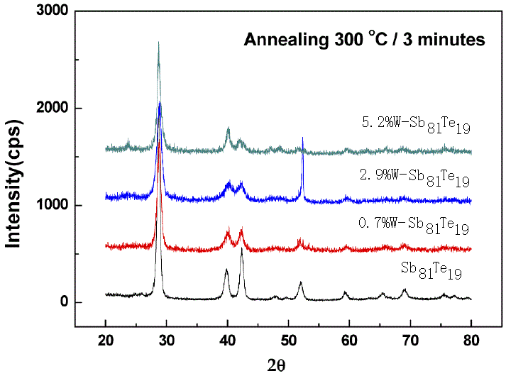 |
|
|
|
|
|
|
132 (for 0% W), 158 (for 0.7% W), 189 (for 2.9% W), and 233 (for 5.2% W) |
536 (for 0% W), 537 (for 0.7% W), 539 (for 2.9% W), and 539 (for 5.2% W) |
|
[47] |
Molten GexSbyTez |
|
|
|
|
 |
|
|
|
 |
Electromigration: Ge and Sb atoms migrate to the cathode, while Te atoms migrate to the anode:
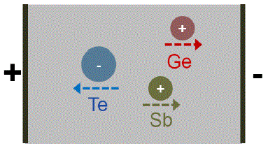 |
[40, 42 - 44] |
Amorphous Ge2Sb2Te5 |
 |
|
|
|
|
|
0.0300 |
|
|
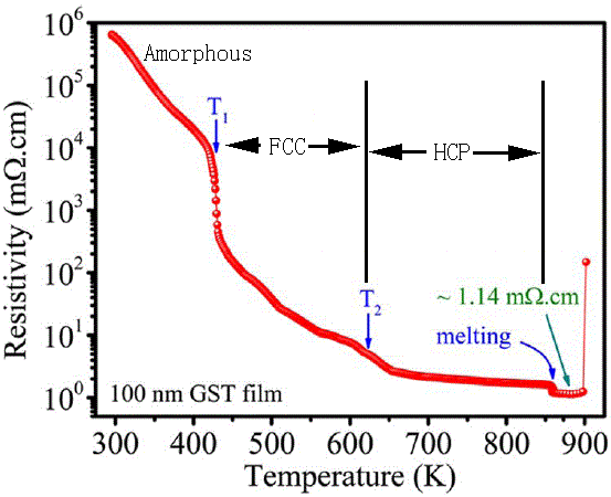
Stable at room temperature for more than 10 years. Both α- and c-Ge2Sb2Te5 can only be etched by nitric acid (HNO3) aqueous solution, but cannot be etched by H2C2O4, HClO4, CH3COOH, H2SO4, H3PO4, HCl; electric conductivity 3 Ω-1-m-1; thermal conductivity 0.2 W/K-m; specific heat 1.25 x 10⁶ J/K-m3; activation energy of crystallization: 3.636 eV; activation energy of structural transformation from fcc to hcp: 1.579 eV; Band gap: 0.7 - 1.0 eV. |
[13, 18, 30, 42, 54] |
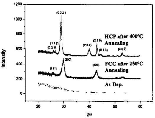
Metastable fcc Ge2Sb2Te5 |
|
|
|
|
a = 0.60 |
0.0335 |
151-174 |
632 |
Metastable phase NaCl-type structure with the Te atoms on one fcc
sublattice and with the Ge and Sb atoms and 20% of vacancies distributed randomly over the other
fcc sublattice; Fm-3m; electric conductivity 2770 Ω-1-m-1; thermal conductivity 0.5 W/K-m; specific heat 1.25 x 10⁶ J/K-m3. |
[5, 9, 17, 42, 45] |
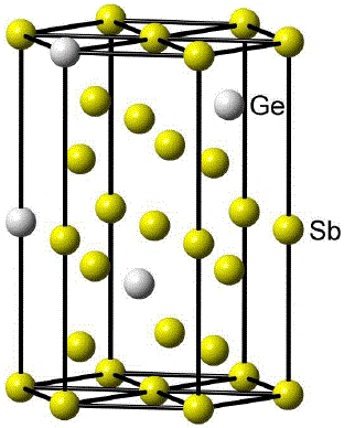
Stable hcp Ge2Sb2Te5 |
 |
|
|
|
a' = 0.425; c' = 1.72 ~ 1.827 |
0.0335 |
151-174 |
632 |
Trigonal cell with stable phase hexagonal structure; (P-3m1); Stacking sequence along the c'-axis of a four layer block of GeTe and one repeat unit
of Sb2Te3: Te–Sb–Te–Ge–Te– Te–Ge–Te–Sb–; thermal conductivity 1.59 W•m-1•K-1, density 6300 kg•m-3, specific heat 1.25 x 10⁶ J/K-m3, Young's modulus 58.7 GPa, thermal expansion coefficient 17.4 × 10⁻⁶ K-1, Poisson's ratio 0.3. |
[4, 6 - 9, 17 - 18, 34 - 37, 42] |
Agx(Ge2Sb2Te5)100-x (x = 0-3 at.%) |
100-x XRD.GIF) |
|
|
|
|
|
|
100-x.GIF) |
|
|
[50] |
Bi-Ge2Sb2Te5 |
|
|
|
|
|
|
|
|
|
|
[52] |
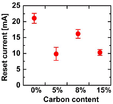
C-Ge2Sb2Te5 |
|
|
|
|
 |
|
|
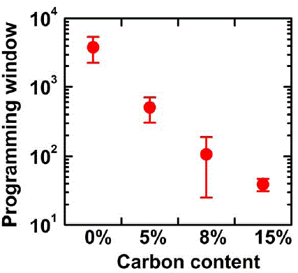
279 (for C5%); 314 (for C8%); 342 (for C15%) |
|
|
[27] |
Co-Ge2Sb2Te5 |
|
|
|
|
|
|
|
|
|
|
[52] |
Cr-Ge2Sb2Te5 |
|
|
|
|
|
|
|
|
|
|
[52] |
Ge-rich GexSbyTez |
 |
|
|
|
 |
|
|
 |
|
|
[39, 41] |
N-Ge2Sb2Te5 |
|
|
|
|
|
|
|
250 (for 15 at.% N)
---------
 |
|
|
[28, 29] |
(Si+N)-Ge2Sb2Te5 |
-Ge2Sb2Te5 b.GIF) |
|
|
|
-Ge2Sb2Te5.GIF) |
|
|
|
|
Crystallization inhibition of GST by SiNx; average grain sizes of pure, Si-, and (Si+N)-GST after 400 °C annealing for 10 min are 20.4, 10.7, and 5.6 nm, respectively. |
[55, 56] |
N-Ge5Sb75Te20 |
 |
|
|
|
|
|
|
|
|
Crystallization time:
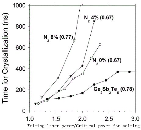 |
[51] |
Fe-Ge2Sb2Te5 |
 |
|
|
|
|
a = 0.4205; c = 1.732 |
|
|
|
UV-visible reflectance spectra:
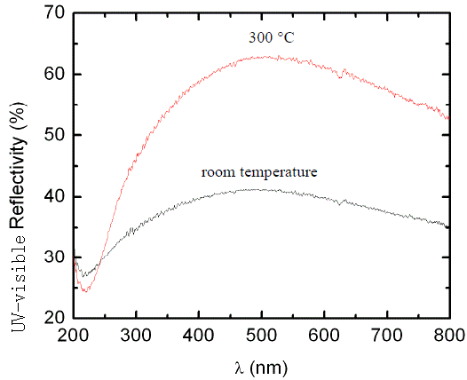 |
[38] |
In-Ge2Sb2Te5 |
|
|
|
|
|
|
|
|
|
|
[52] |
O-Ge2Sb2Te5 |
 |
|
|
|
|
|
|
|
|
|
[45] |
Pb-Ge2Sb2Te5 |
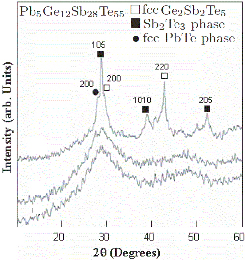 |
|
|
|
|
|
|
Increases with higher Pb at%: 124 - 138 |
|
|
[52, 53] |
Sb-Ge2Sb2Te5 |
|
|
|
|
|
|
|
|
|
Conductive Sb filaments with electrical current are formed due to excess Sb atoms. |
[58] |
Sn-Ge2Sb2Te5 |
 |
|
|
|
|
|
|
|
|
|
[49] |
Ti-Ge2Sb2Te5 |
|
|
|
|
|
|
|
|
|
|
[52] |
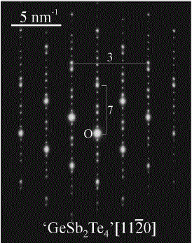
GexSb2Te3+x |
|
|
|
|
|
|
|
|
|
An alternation in
c'-axis of one repeat unit of Sb2Te3 and a block consisting
of 2x layers GeTe |
[6] |
Amorphous GeSb2Te4 |
|
|
|
Asymmetrical tetrahedral structure:
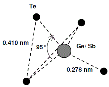 |
|
|
0.0304 |
|
|
Bond length: Ge(Sb)-Te = 0.278±0.004 nm; Te-Te = 0.410±0.004 nm (shorter than in the corrsponding crystalline phases). Bond angle: Te-Ge-Te = 95°. |
[17] |
Metastable cubic GeSb2Te4 |
|
|
|
|
|
|
0.0316 |
|
|
Bond length: Ge(Sb)-Te = 0.295±0.004 nm; Te-Te = 0.417±0.004 nm. Bond angle: Te-Ge-Te = 90°. |
[17] |
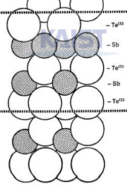
Stable hexagonal GeSb2Te4 |
|
 |
|
|
|
a' = 0.425; c' = 4.10 |
0331 |
|
|
The periodicity is 21:
-Te-Ge-Te-Sb-Te-vac-Te-Sb-Te-Ge-Te-Sb-Te-vac-Te-Sb-Te-Ge-Te-Sb-Te-vac-Te-Sb-. Very high static dielectric constant 98. |
[6 - 8, 14, 15, 17] |
O-GeSb2Te4 |
 |
|
|
|
|
|
|
|
|
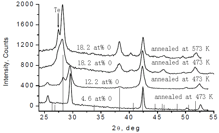
For O < 10 at.%, Te, Sb and most of Ge are in metallic state, and free O is located at tetrahedral interstitial sites and acts as nucleation center; Higher O at.%, segregated Te is in metallic state; Higher T (573 K) promoted Te phase. |
[48] |
GeSb4Te7 |
|
|
|
|
3.47 X 10⁻⁴ Ω•m; |
|
|
|
|
Thermal conductivity 0.49 W•m-1•K-1, specific heat 193.55 J•kg-1•K-1, density 5685
kg•m-3 Young's modulus 37.8 GPa, thermal expansion coefficient 17.913 × 10⁻⁶ K-1, Poisson's ratio 0.3. |
[32 - 34] |
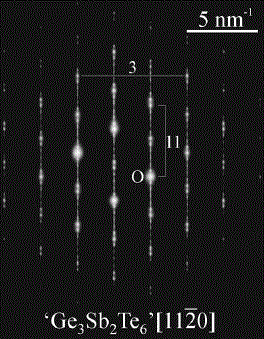
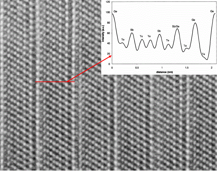
Ge3Sb2Te6 |
|
 |
 |
|
|
a' = 0.425; c' = 6.26 |
|
|
|
|
[6 - 8] |
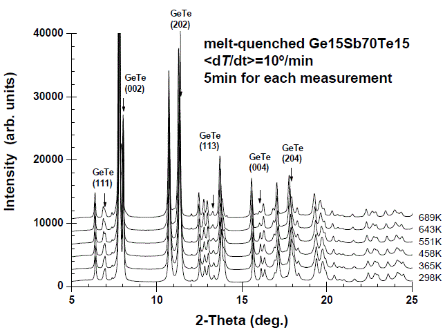
Ge15Sb70Te15 |
 |
|
|
|
|
|
|
|
|
Space group R-3m; |
[12] |
Diamond-type Ge |
|
|
|
|
|
a = 0.565735 at 20 °C |
|
|
|
Fd-3m |
[10, 11] |
Ge15Sb85 |
|
|
|
|
|
|
|
|
|
|
[13] |
(O+N)-Ge21Sb26Te53 |
|
|
|
|
|
|
|
-Ge21Sb26Te53.GIF) |
|
|
[57] |
InSb |
|
|
|
|
|
|
|
168 |
490 |
|
|
InSbTe |
|
|
|
|
|
|
|
200 |
500-600 |
|
|
In3SbTe2 |
|
|
|
|
|
|
0.0351 |
|
|
|
[13, 21] |
In10GexSb52-xSn23Te15 |
|
|
|
|
|
|
|
192.6 (for x = 2); 201.5 (for x = 5); 208.6 (for x = 7); 213.1 (for x = 9). |
|
|
[25] |
InSe |
|
|
|
|
|
|
|
200 & 650 |
890 |
|
|
Ga3Sb8Te |
|
|
|
|
|
|
|
227 |
567.5 |
|
[23] |
Si3.9Sb45.6Te50.5 |
|
|
|
|
|
|
|
180 |
550 |
|
[24] |
Si-Ga2TeSb7 |
 |
|
|
|
|
|
|
260–361 (increase with
increasing Si-composition) |
|
|
[26] |
Te81Ge15Sb2S2 |
|
|
|
|
|
|
|
|
380 |
|
|
TeGa2Sb14 |
|
|
|
|
|
|
|
232 |
584 |
Activation energy
of crystallization 3.66 eV; |
[22] |
Note that for GexSbyTez, a higher vacancy concentration results in a higher crystallization speed. [31] The elemental concentrations of GexSbyTez are normally quantified by using EDS measurements with Ge K, Sb L, and Te L lines. [46]
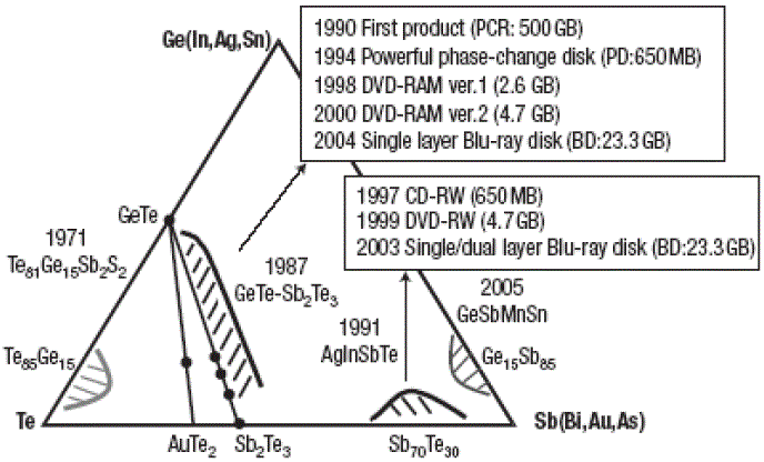
Figure 3161a. Application of GST alloys for optical storage. [60]
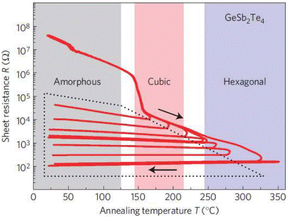
Figure 3161b shows the dependence of crystallized fraction of amorphous Ge2Sb2Te5 (GST) on the annealing time and temperature.
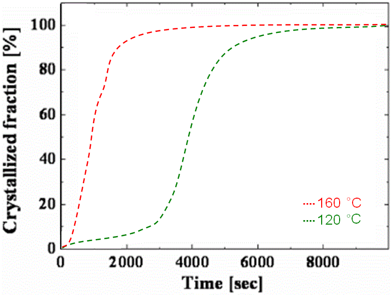
Figure 3161b. Dependence of crystallized fraction of amorphous Ge 2Sb 2Te 5 (GST) on the annealing time and temperature. |
[1] Structure Reports, edited by W. P. Pearson (International Union of Crystallography, New York, 1953), Vol. 17, p. 44.
[2] J. Goldak, C. S. Barrett, D. Innes, and W. Youdelis, J. Chem. Phys. 44, 3323 (1966).
[3] R. W. G. Wyckoff, Crystal Structures, 2nd ed. (Interscience, New York, 1963), Vol. 2, pp. 29–31.
[4] I. I. Petrov, R. M. Imamov, and Z. G. Pinsker, Sov. Phys. Crystallogr. 13, 339 (1968).
[5] N. Yamada and T. Matsunaga, J. Appl. Phys. 88, 7020 (2000).
[6] B. J. Kooi and J. Th. M. De Hosson, Electron diffraction and high-resolution transmission electron microscopy of the high temperature crystal structures of GexSb2Te3+x (x = 1, 2, 3
) phase change material, J. Appl. Phys.92 (7), 3584 (2002).
[7] V. Weidenhof, I. Friedrich, S. Ziegler, and M. Wuttig, J. Appl. Phys. 86, 5879 (1999).
[8] I. I. Petrov, R. M. Imamov, and Z. G. Pinsker, Sov. Phys. Crystallogr. 13, 339 (1968).
[9] Fei Yang, Ling Xu, Rui Zhang, Lei Geng, Liang Tong, Jun Xu, Weining Su, Yao Yu, Zhongyuan Ma, Kunji Chen, Direct observation of phase transition of GeSbTe thin films by Atomic Force Microscope, Applied Surface Science 258 (2012) 9751– 9755.
[10] Edited by T. Hahn: International Tables for Crystallography, Vol. A (Kluwer, Dordrecht, 1995).
[11] R W. G. Wyckoff: Crystal Structures, Vol. 1 (Interscience, New York, 1963).
[12] Toshiyuki Matsunaga, Rie Kojima, Noboru Yamada, Kouichi Kifune, Yoshiki Kubota, Sinji Kohara, Structural investigation of Sb-based phase-change materials.
[13] Wei Zhang, Ab Initio Investigation of Phase Change Materials: Structural, Electronic and Kinetic properties,
Master thesis, 2014.
[14] Siegrist T, Jost P, Volker H, Woda M, Merkelbach P, Schlockermann C, et al.
Disorder-induced localization in crystalline phase-change materials. Nature materials 2011,
10(3): 202-208.
[15] Lencer D. Design Rules, Local Structure and Lattice-Dynamics of Phase-Change Materials for
Data Storage Applications. PhD thesis, RWTH Aachen 2010.
[16] Dove DB. Short-range order in amorphous GeTe films. Applied Physics Letters 1970, 16(3):138.
[17] Boyn S. Elektrische und optische Eigenschaften von kristallinen pseudo-binaeren GeSbTe
Phasenwechselmaterialien. Bachelor thesis, RWTH Aachen 2009.
[18] Njoroge WK , Woltgens H -W, Wuttig M. Density changes upon crystallization of Ge2Sb2.04Te4.74 films. Journal of Vacuum Science & Technology A: Vacuum, Surfaces, and
Films 2002, 20(1): 230.
[19] Anderson TL, Krause HB. Refinement of the Sb2Te3 and Sb2Te2Se structures and their
relationship to nonstoichiometric Sb2Te3-ySey compounds. Acta Crystallogr B 1974 30 1307.
[20] Njoroge W. Phase Change Optical Recording - Preparation and X-ray Characterization of
GeSbTe and AgInSbTe film. PhD thesis, RWTH Aachen 2001.
[21] Zalden P. Phase-Change Materials Structure, vibrational states and thermodynamics of
crystallization. PhD thesis, RWTH Aachen 2012.
[22] Yung-Ching Chu, Chien-Tu Chao, Po-Chin Chang, Shih-Ching Chang, Jong-Ching Wu, and Tsung-Shune Chin, Characteristics of TeGa2Sb14 Thin Films for Phase-Change Memory, IEEE Transactions on Magnetics, 47(3), 637 2011.
[23] C. M. Lee, Y. I. Lin, and T. S. Chin, Crystallization kinetics
of amorphous Ga–Sb–Te chalcogenide films, J. Mater. Res, vol.
19, 2929 (2004).
[24] Yuta Saito, Yun Heub Song, Member, IEEE, Jung Min Lee, Yuji Sutou, and Junichi Koike, Multiresistance Characteristics of PCRAM With Ge1Cu2Te3 and Ge2Sb2Te5 Films, IEEE Electron Device Letters, 33 (10), 1399 (2012).
[25] Sin Liang Ou, Kuo Sheng Kao, Chao Te Lee, Tsung Shine Ko, Han Feng Chang, and Huan Hsien Yeh, Recording Characteristics and Crystallization Behavior of InGeSbSnTe Phase Change Thin Films, IEEE Transactions on Magnetics, 50(7), 3501604, 2014.
[26] Alfred Tung Hua Chuang, Yi-Chou Chen, Yung-Ching Chu, Po-Chin Chang, Kin-Fu Kao, Chih-Chung Chang, Kuang-Yeu Hsieh, Tsung-Shune Chin, Chih-Yuan Lu, Temperature Robust Phase Change Memory using Quaternary Material System based on Ga2TeSb7, DOI: 10.1109/IMW.2011.5873240, 2011.
[27] Q. Hubert, C. Jahan, A. Toffoli, G. Navarro, S. Chandrashekar, P. Noé, D. Blachier, V. Sousa, L. Perniola, JF. Nodin, A. Persico, R. Kies, S. Maitrejean, A. Roule, E. Henaff, M. Tessaire, P. Zuliani, R. Annunziata, G. Pananakakis, G. Reimbold, B. De Salvo, Lowering the reset current and power consumption of Phase-Change Memories with carbon-doped Ge2Sb2Te5, DOI:10.1109/IMW.2012.6213683 (2012).
[28] Chun Chia Tan, Rong Zhao, Luping Shi, Tow Chong Chong, James A. Bain, T. E. Schlesinger, Jonathan A. Malen, Wee Liat Ong, Thermal Conductivity Measurements of Nitrogen doped Ge2Sb2Te5, DOI:10.1109/NVMTS.2011.6137080, 2011 11th Annual Non-Volatile Memory Technology Symposium (NVMTS), 2011.
[29] Hun Seo et al., Investigation of crystallization behavior of sputter-deposited nitrogen-doped amorphous Ge2Sb2Te5 thin films, Jpn. J. Appl. Phys, 39, 745, 2000.
[30] Huai-Yu Cheng, Chao-An Jong, Chain-Ming Lee, and Tsung-Shune Chin, Wet-Etching Characteristics of Ge2Sb2Te5 Thin
Films for Phase-Change Memory, IEEE Transactions on Magnetics, 41(2) 1031, 2005.
[31] Wuttig, M., et. al., “The role of vacancies and local distortions in the design of new phase-change materials”, Nature Materials, Vol 6, February 2007, p. 122.
[32] S. Shin, H. K. Kim, J. Song, D. J. Choi, and H. H. Cho, “Phase-dependent
thermal conductivity of Ge1Sb4Te7 and N:Ge1Sb4Te7 for phase change
memory applications,” J. Appl. Phys., vol. 107, no. 3, pp. 033518-1, Feb. 2010.
[33] H. K. Kim, S. Y. Lee, D. J. Choi, S. Shin, H. H. Cho, and J. S. Roh,
“Effects of nitrogen doping and working pressure on the crystallization
of Ge1Sb4Te7 thin films for PRAM applications,” J. Korean Phys. Soc.,
vol. 55, no. 5, pp. 1896–1900, Nov. 2009.
[34] S. S. Kim, S. M. Jeong, K. H. Lee, Y. K. Park, Y. T. Kim, J. T. Kong,
and H. L. Lee, “Simulation for reset operation of Ge2Sb2Te5 phasechange random access memory,” Jpn. J. Appl. Phys. 2, Lett., vol. 44, no. 8,
pp. 5943–5948, Aug. 2005.
[35] H.-K. Lyeo, D. G. Cahill, B.-S. Lee, J. R. Abelson, M.-H. Kwon,
K.-B. Kim, S. G. Bishop, and B.-K. Cheong, “Thermal conductivity of
phase-change material Ge2Sb2Te5,” Appl. Phys. Lett., vol. 89, no. 15,
pp. 151904-1–151904-3, Oct. 2006.
[36] S. M. Sadeghipour, L. Pileggi, and M. Asheghi, “Phase change random
access memory, thermal analysis,” in Proc. ITHERM, 2006, pp. 660–665.
[37] I.-M. Park, J.-K. Jung, S.-O. Ryu, K.-J. Choi, B.-G. Yu, Y.-B. Park,
S. M. Han, and Y.-C. Joo, “Thermomechanical properties and mechanical
stresses of Ge2Sb2Te5 films in phase-change random access memory,”
Thin Solid Films, vol. 517, no. 2, pp. 848–852, Nov. 2008.
[38] J. C. Huang, W. D. Song, L. P. Shi, R. Zhao, T. C. Chong, J. A. Bain, T. E. Schlesinger, Crystallinity and its Influence on Physical and Magnetic Properties in Phase Change Magnetic Materials, 2011 11th Annual Non-Volatile Memory Technology Symposium (NVMTS), DOI:10.1109/NVMTS.2011.6137109, (2011).
[39] Nicola Ciocchini, Elisabetta Palumbo, Massimo Borghi, Paola Zuliani, Roberto Annunziata, Daniele Ielmini, Modeling Resistance Instabilities of Set and Reset States in Phase Change Memory with Ge-Rich GeSbTe, IEEE Transactions on Electron Devices, 61(6) 2136 (2014).
[40] Young-Chang Joo, Tae-Youl Yang, Ju-Young Cho, and Yong-Jin Park, Electromigration in Molten-phase Ge2Sb2Te5 and
Effects of Doping on Atomic Migration Rate, Journal of the Korean Ceramic Society, 49(1), pp. 43~47, 2012.
[41] Paola Zuliani, Enrico Varesi, Elisabetta Palumbo, Massimo Borghi, Innocenzo Tortorelli, Davide Erbetta, Giovanna Dalla Libera, Nicola Pessina, Anna Gandolfo, Carlo Prelini, Leonardo Ravazzi, and Roberto Annunziata, Overcoming Temperature Limitations in Phase Change Memories with Optimized GexSbyTez, IEEE Transactions on Electron Devices, 60(12), 4020 (2013).
[42] Kadir Cil, Faruk Dirisaglik, Lhacene Adnane, Maren Wennberg, Adrienne King, Azer Faraclas, Mustafa B. Akbulut, Yu Zhu, Chung Lam, Ali Gokirmak, and Helena Silva, Electrical Resistivity of Liquid Ge2Sb2Te5 Based on Thin-Film and Nanoscale Device Measurements, IEEE Transactions on Electron Devices, 60(1), 433 (2013).
[43] Mattia Boniardi, Andrea Redaelli, Innocenzo Tortorelli, Simone Lavizzari, Agostino Pirovano, Fabio Pellizzer, Enrico
Varesi, Davide Erbetta, Camillo Bresolin, Alberto Modelli and Roberto Bez, Electrical and Thermal Behavior of Tellurium poor GeSbTe compounds for Phase Change Memory, 2012 4th IEEE International Memory Workshop (IMW), DOI:10.1109/IMW.2012.6213679, (2012).
[44] Tae-Youl Yang, Ju-Young Cho, Yong-Jin Park, and Young-Chang Joo, Effects of dopings on the electric-field-induced
atomic migration and void formation in Ge2Sb2Te5, 2011 18th IEEE International Symposium on the Physical and Failure Analysis of Integrated Circuits (IPFA), DOI:10.1109/IPFA.2011.5992717, (2011).
[45] Shin Kikuchi, Dong Young Oh, Isao Kimura, Yutaka Nishioka, Masahisa Ueda, Mitsuhiro Endo, Yutaka Kokaze and
Koukou Suu, Preparation of Oxygen-doped and Nitrogen-doped Ge-Sb-Te System Thin Film for Phase Change Random Access Memory by RF Magnetron Sputtering, 7th Annual Non-Volatile Memory Technology Symposium, NVMTS, DOI:10.1109/NVMT.2006.378882, 2006.
[46] Kai-Liang Zhang, Qi-Bin Liu, Zhi-Tang Song, Song-Lin Feng, Bomy Chen, Study on Chemical Mechanical Polishing of GeSbTe for Chalcogenide Phase Change Memory, ICSICT '06. 8th International Conference on Solid-State and Integrated Circuit Technology, DOI:10.1109/ICSICT.2006.306518, 2006.
[47] Kin-Fu Kao, Huai-Yu Cheng, Chao-An Jong, Chi-Jui Lan, and Tsung-Shune Chin, Tungsten Added Sb80Te20 for Phase-Change RAM, IEEE Transactions on Magnetics, 43(2), 930, 2007.
[48] E. Morales-Sánchez, J. González-Hernández, P. Herrera-Fierro , B. Chao, Yu. Kovalenko, E. Prokhorov, Influence of oxygen on the crystallization process in Ge:Sb:Te:O films, 2006 3rd International Conference on Electrical and Electronics Engineering, DOI:10.1109/ICEEE.2006.251847, (2006).
[49] Y. C. Chen, C. T. Chen, J. Y. Yu, C.Y. Lee, C. F. Chen, S. L. Lung, and Rich Liu, 180nm Sn-Doped GezSbtTes Chalcogenide Phasechange Memory Device for Low Power, High Speed Embedded Memory for SoC Applications,
DOI:10.1109/CICC.2003.1249426, Proceedings of the IEEE 2003 Custom Integrated Circuits Conference, 2003.
[50] C. T. Lie, P. C. Kuo, T. H. Wu, and P. W. Chen, Ge2Sb2Te5 Thin Film Doped with Silver, International Symposium on Optical Memory and Optical Data Storage Topical Meeting, DOI:10.1109/OMODS.2002.1028619, 2002.
[51] Byung-ki Cheong, In Ho Kim, Hanju Jung, Taek Sung Lee, Jeung-hyun Jeong, Dae-Hwan Kang, Won Mok Kim, and Jae-Geun Ha, Effects of Nitrogen Addition on the Properties of Ge-Doped SbTe Phase Change
Memory Material, Electronic Materials Letters, Vol. 2, No. 1 (2006), pp. 43-48.
[52] J. Kumar, P. Kumar, M. Ahmad, R. Chander, R. Thangaraj, and T.S. Sathiaraj, Phase transformation in Pb:GeSbTe chalcogenide films, DOI: 10.1051/epjap:2008165, Eur. Phys. J. Appl. Phys. 44, 117–123 (2008).
[53] J. Kumar, M. Ahmad, R. Chander, R. Thangaraj, and T.S. Sathiaraj, Phase segregation in Pb:GeSbTe chalcogenide system, DOI: 10.1051/epjap:2007173, Eur. Phys. J. Appl. Phys. 41, 13–18 (2008).
[54] Baowei QIAO,Yunfeng LAI,Jie FENG,Yun LING,Yinyin LIN,Ting'ao TANG,Bingchu CAI,Bomy CHEN,
Bomy,CHEN, study of Ge2Sb2Te5 film for nonvolatile memory medium, J. Mater. Sci. Technol. 21(1) 95, 2005.
[55] Cai Yan-Fei, Zhou Peng, Lin Yin-Yin, Tang Ting-Ao, Chen Liang-Yao, Li Jing, Qiao Bao-Wei, Lai Yun-Feng, Feng Jie, Cai Bing-Chu and Chen Bomy, Nitrogen and Silicon Co-Doping of Ge2Sb2Te5 Thin Films for Improving Phase Change Memory Performance, Chinese Phys. Lett. 24 781 doi:10.1088/0256-307X/24/3/053, 2007.
[56] Lai Y F et al. J. Electron. Mater. 34, 176, (2005).
[57] D. Dimitrov, H.-P.D. Shieh, The influence of oxygen and nitrogen doping on GeSbTe
phase-change optical recording media properties, Materials Science and Engineering B107 (2004) 107–112.
[58] Ramanathaswamy Pandian, Bart J. Kooi, Jasper L. M. Oosthoek, Pim van den Dool, George Palasantzas, and Andrew Pauza, Polarity-dependent resistance switching in GeSbTe phase-change thin films: The importance of excess Sb in filament formation, Applied Physics Letters 95, 252109 (2009).
[59] Vorgelegt Von, Quantitative TEM analysis of crystalline and amorphous GeTe-based chalcogenides, M.Sc. thesis, (2009).
[60] M. Wuttig, Nature Materials 6 (2007) 824-832.
[61] I. Friedrich, W. K. Njoroge, P. Franz, and M. Wuttig, J.Appl. Phys., Vol.87, No.9 (2000) 4130-4134.
[62] W. Welnic et al., Nature Materials 5 (2006) 56-62.
[63] Giovanni Betti Beneventi, Characterization and modeling of phase-change
memories, thesis, 2012.
|


100-x XRD.GIF)
100-x.GIF)


-Ge2Sb2Te5 b.GIF)
-Ge2Sb2Te5.GIF)


-Ge21Sb26Te53.GIF)