=================================================================================
SrTiO3 has cubic perovskite crystalline structure and is a band insulator with an empty d band. The titanium valence in SrTiO3 is 4+. The lattice constant for SrTiO3 is 3.91 Å.
The sandwich structure shown in Figure 3520a (a) is composed of three layers: SrTiO3, PbTiO3, and Pt. An amorphous Ti-rich interfacial layer as well as nanometer size precipitates was formed at PbTiO3/Pt interfaces. In the low-loss region in EELS from the different layers shown in Figure 3520a (b), the energy peaks labeled A–H for SrTiO3 and a–h for PbTiO3 are formed by interband transitions which are typical in bulk SrTiO3 and PbTiO3 [1]. The strong peaks H/h and H’/h’ arise from transitions of Ti 3p to higher energy levels such as Ti 3d, Ti 4s, forming Ti M2,3 edge. In the precipitates, the transitions h and h are reduced in intensity because these precipitates might be Ti-deficient. In Figure 3520a (c), the two core loss EELS profiles from SrTiO3 and PbTiO3 layers show clear splitting of the Ti-L2,3 edges, while for the interfacial layer the splitting at the Ti-L3 edge is much less and the splitting at the Ti-L2 edge disappears. The splitting of Ti-L2,3 edges reflects the hybridization and ligand field strength of Ti–O atomic interaction so that the reduction of splitting in the interfacial layer reflects the weaker Ti–O bonding force. Due to the similar hybridization of O 2p states with Ti 3d in the conduction band, the energy region from 530 eV to 536 eV is split into two subbands t2g (marked peak 1) and eg (marked peak 2). Figure 3520a (d) shows the EEL spectra of Pb- and Pt-M4,5 edges.
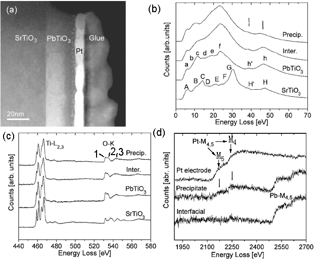
Figure 3520a. (a) TEM image of sandwich structure ( SrTiO3, PbTiO3, and Pt), and (b) low-loss region in EELS, (c) Ti-L2,3 and O-K edges, and (d) Pb- and Pt-M4,5 edges
from the different layers. The black arrows in (d) denote the positions of Pt-M4,5 edges. Adapted from [2]
In EELS, perovskite type ferroelectric and high-k dielectric materials, such as BaTiO3 and SrTiO3, normally show only one interband plasmon peak [3–6].
Table 3520. Properties of SrTiO3.
Figure 3520b shows a STEM Z-contrast image of an 8° [0 0 1] tilt grain boundary in SrTiO3 in the [0 0 1] orientation, indicating two adjacent grains with cubic symmetry and five dislocation cores (dark ovals) at the grain boundary. Figure 3520b (b) shows one of the dislocation cores at a higher magnification. The brighter columns surrounding the core represent the Sr columns, while the less bright columns represent the Ti–O columns. Due to the small scattering amplitude of oxygen, the pure O columns are not visible.
![Z-contrast image of a 8° [0 0 1] tilt grain boundary in SrTiO3](image1/3520b.jpg)
Figure 3520b. (a) Z-contrast image of a 8° [0 0 1] tilt grain boundary in SrTiO3, and (b) One of the dislocation cores at a higher magnification. [7]
Artifacts in high resolution HAADF STEM imaging can be induced if the specimen is too thick. For instance, Figure 3520c shows high resolution STEM ADF images taken from (001) SrTiO3 single crystals in different specimen thicknesses (t). The ADF lattice periodicity of the specimen in the thickness of t/λ=6 does not represent the periodicity of the crystal potential, indicating there is an imaging artifact when the specimen is too thick.
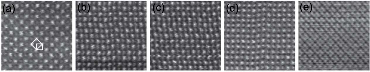
Figure 3520c. High resolution STEM ADF images taken from (001) SrTiO3 single crystals as a function of crystal thickness: (a) t/λ = 0.25, (b) =0.5, (c) = 0.9, (d) = 1.2, (e) =6. λ is the mean free path (λ = ~115 nm for SrTiO3) and ADF collection angle here was 46–104 mrad.
Adapted from [8]
It should be highlighted that the ADF contrast maximum did not occur at the thinnest area but at t/λ = 0.9. They [8] suggested the reason for that is there was a surface amorphous layer on the specimen. Therefore, in very thin regions, the fraction of the crystal is small comparing with that of amorphous surface, resulting in lower image contrast.
Figure 3520d shows the contrast of high resolution HAADF STEM image, as a function of crystal tilt from 0° to 4° (0-67 mrad), taken from a (100) SrTiO3 crystal in Cs-corrected STEM mode. A small crystal tilt (e.g. 0-15 mrad) can reduce the contrast of high resolution ADF images by a factor of 2 because of dynamical scattering. Moreover, this effect also depends on the sample thickness, which was 15 nm here.
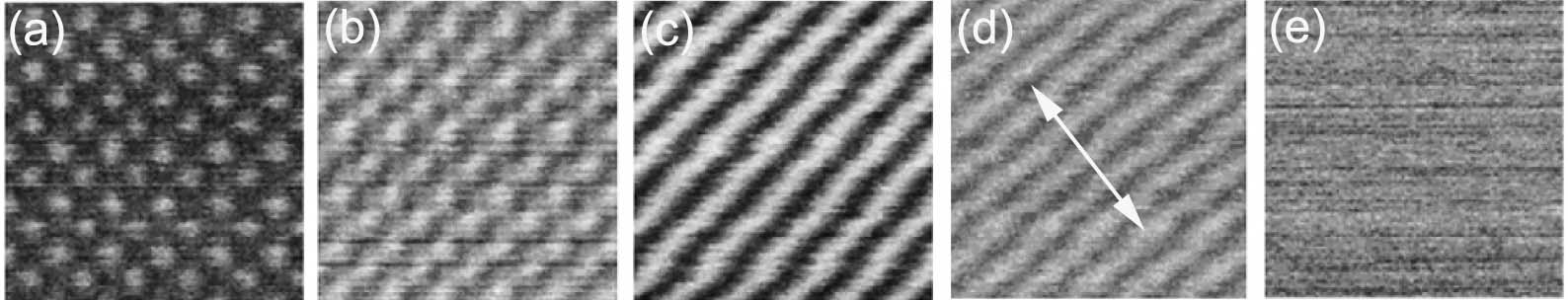
Figure 3520d. STEM-ADF image of (100) SrTiO3 as a function of crystal tilt. (a) 0°; (b) 1°; (c) 2°; (d) 3°; and (e) 4°. The tilt axis as marked in (d) is near the [110]. Adapted from [8]
Except for Ni/YSZ as the most common anode material in SOFCs, gadolinium doped ceria oxide (GDC), doped SrTiO3 [9,10], and Cu-CeO-YSZ [11] are also used. Nonetheless, some of them have disadvantages of complicated fabrication processes, low conductivity or poor electrochemical catalyst activity.
Figure 3520e shows the temperature-composition phase diagram of (Ba1-xSrx)TiO3.
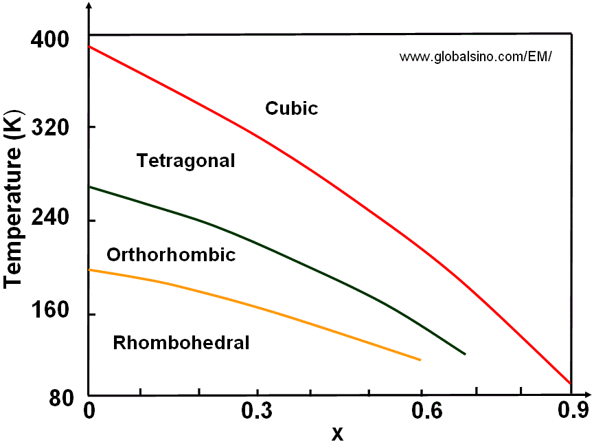
Figure 3520e. Temperature-composition phase diagram of (Ba1-xSrx)TiO3.
[1] K. V. Benthem, C. Elsasser, and R. H. French, J. Appl. Phys. 90, 6156 (2001).
[2]
L. F. Fu, S. J. Welz, and N. D. Browning, M. Kurasawa, and P. C. McIntyre, Z-contrast and electron energy loss spectroscopy study of passive layer formation at ferroelectric PbTiO3/Pt interfaces, Applied Physics Letters, 87, 262904 (2005).
[3] K.S. Katti, M. Qian, F. Dogan, M. Sarikaya, J. Am. Ceram. Soc. 85 (2002)
2236–2243.
[4] K. van Benthem, C. Elsasser, R.H. French, J. Appl. Phys. 90 (2001) 6156–6164.
[5] S. Schamm, G. Zanchi, Ultramicroscopy 88 (2001) 211–217.
[6] J. Zhang, A. Visinoiu, F. Heyroth, F. Syrowatka, M. Alexe, D. Hesse, H.S. Leipner,
Phys. Rev. B 71 (2005) 064108.
[7] R.F. Klie, I. Arslan, N.D. Browning, Atomic resolution electron energy-loss spectroscopy, Journal of Electron Spectroscopy and Related Phenomena 143 (2005) 105–115.
[8] H. Inada, D.Su, R. F. Egerton, M.Konno, L.Wu, J.Ciston, J.Wall, Y.Zhu, Atomic imaging using secondary electrons in a scanning transmission electron microscope: Experimental observations and possible mechanisms, Ultramicroscopy 111(2011)865–876.
[9] J. Canales-Vazquez, S.W Tao, J.T.S Irvine, Solid State Ionics, 2003. 159(1–2): p. 159-165.
[10] S. Hui, A. Petric, Journal of The Electrochemical Society, 2002. 149(1): p. J1-J10.
[11] S. Park, J.M. Vohs, R.J. Gorte, Nature, 2000. 404(6775): p. 265-267.
|