=================================================================================
Table 4461a. Progress of novel TEM developments in times.
Focus |
Developments |
Time |
Spatial resolution |
No compromise in spatial resolution:
new pole piece design yields increased EDS solid angle without sacrificing resolution |
2020 |
Updated CCD |
Charge
coupled device (CCD) detectors now enables the collection of energy-filtered images with
nearly single-electron sensitivity, which minimizes the statistical noise in the elemental maps [5] |
1998 |
Updated design of energy filters |
Improvements in the design of energy filters provide a high degree of
isochromaticity over large image sizes, leading to reduced systematic errors in signal estimation [6-7] |
1995-2004 |
Flexible control of data acquisition |
Flexible control of the data acquisition with user-defined computer
scripts enables more functions or automations [9-10]
|
1999-now |
Environmental effects |
Mitigation of environmental effects:
new enclosure reduces impact of air flow, temperature changes, and acoustic noise |
2020 |
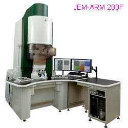
| Modern TEM can achieve very high spatial resolutions. For example, JEM-ARM 200F TEM has been integrated with aberration correction into a super-shielded electron column that safeguards the ultrahigh-powered optics from environmental interferences. The completely new electron column design in this type of microscopes provides atomic spatial energy resolution as well as high probe currents (e.g. high intensities) to increase the signal-to-noise ratio of recorded images, enabling both atom-by-atom imaging resolution and unmatched spatial resolution for atom-to-atom chemical mapping of robust materials, including EDS and EELS, and low-dose STEM imaging for biological applications. Figure 4461a shows the resolved Si (silicon) structures by UT-SA JEOL JEM-ARM 200F. Figure 4461a (b) demonstrates that HAADF image gave at least 78 picometer spatial resolution. Clearly, these high resolution microscopes can be used for sub-atomic research. |
 |
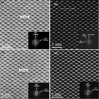
| Figure 4461a. (a-b) Bright field (BF) and HAADF STEM images of Si [110] taken at 200 kV on JEOL JEM-ARM 200F. The HAADF image shows spatial resolution down to 0.078 nm, while the BF image resolves spatial information < 0.1 nm. (c-d) Bright field (BF) and HAADF STEM images of Si [110] taken at 120 kV on JEOL JEM-ARM 200F. Both the HAADF and BF images show spatial resolution down to < 0.1 nm. |
Table 4461b lists examples of advanced aberration-corrected STEM systems which have been reported recently. For instance, it was reported [1] that aberrations up to the fifth-order were successfully measured using an autocorrelation function of the segmental areas of a Ronchigram in a 300-kV STEM. The Ronchigram had an infinite magnification area with a half-angle of 50 mrad, corresponding to the convergence angle of the uniform phase.
Table 4461b. Examples of advanced aberration-corrected STEM systems.
| Accelerating voltage |
Half-angle of infinite magnification area (after correction) |
Correction method |
Highest aberration corrected |
Formed spot size after correction |
Reference |
| 300 kV |
50 mrad |
Ronchigram |
Fifth-order |
|
[1] |
| 300 kV |
40 mrad |
|
|
≤ 50 pm |
[2] |
Von Harrach et al. [3] in FEI Company presented an advanced EDS detector for an FEI 200kV TEM/STEM system. In their system, the EDS detector, consisting of multiple windowless SDDs, had been integrated and placed symmetrically around the electron beam axis in the objective lens chamber without affecting the S/TEM resolution. The total active area of the SDDs was 120 mm2, designed by PN Sensor. The front-end electronics and ultra fast multi-channel pulse processor were provided by Bruker AXS MA. The processor was capable of fast mapping with pixel dwell times down to a few microseconds and >100 kcps count rates per channel. Figure 4461b shows the comparison of the relative MDMs (minimum detectable masses), obtained from 50 nm SrTiO3 TEM specimen, versus analysis time t by EDS with a Si(Li) detector and the 120 mm2 SDD detector, and by EELS. This large SDD detector even provided better MDM than that of EELS. Furthermore, in general, the techniques are more sensitive to the elements if the detection time is longer.
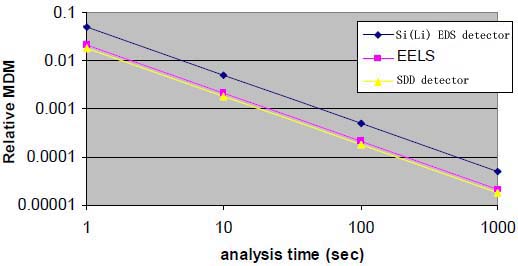
Figure 4461b. Comparison of the relative MDMs, obtained from 50 nm SrTiO3 TEM specimen, versus analysis time t by EDS with a Si(Li) detector and the 120 mm2 SDD detector, and by EELS. Adapted from [3]
Ion pumps are often directly added to the specimen stage (especially for analytical EMs) or gun chambers of EMs to enhance the vacuum in these important regions.
Figures 4461c and 4461d show the most powerful TEM ever made, which is Hitachi 3 MeV, and the 1 MeV Atomic Resolution Microscope (ARM) at the Lawrence Berkeley Laboratory, respectively.
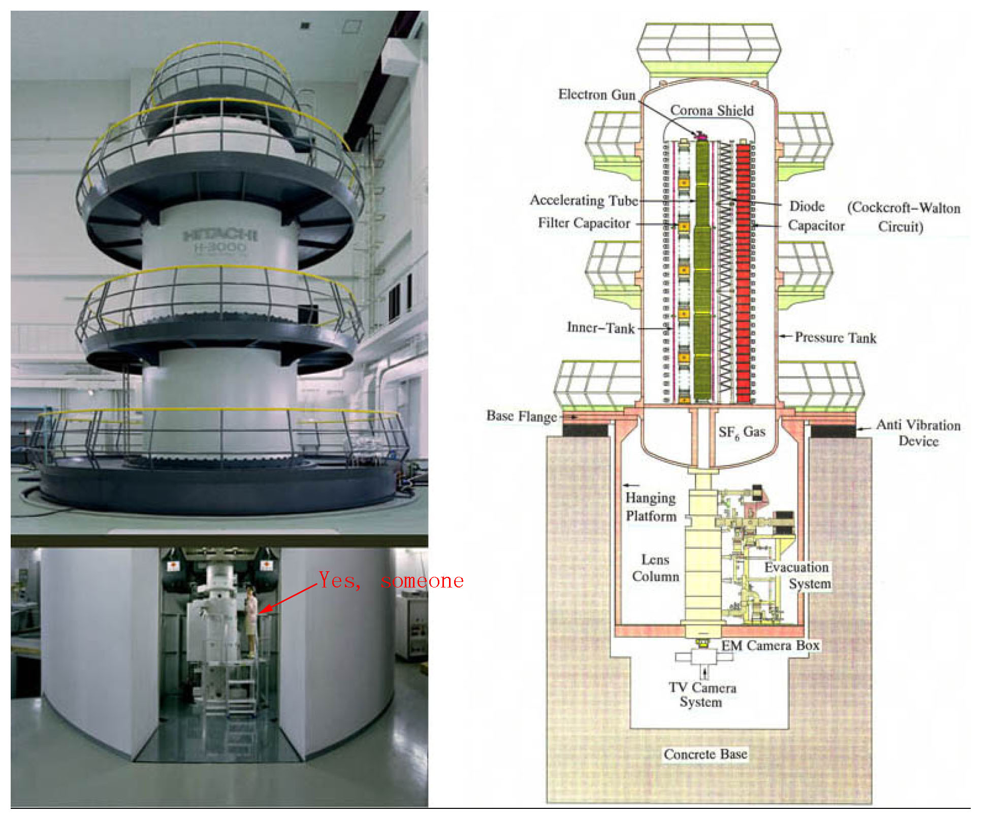
Figure 4461c. Hitachi 3 MeV: the most powerful TEM ever made.
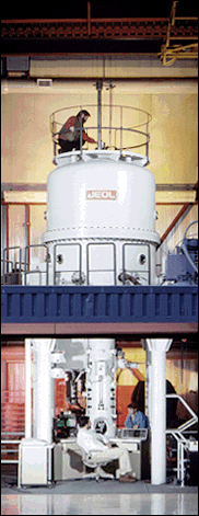
Figure 4461d. The 1 MeV Atomic Resolution Microscope (ARM) at the Lawrence Berkeley Laboratory [4].
[1] H. Sawada, T. Sannomiya, F. Hosokawa, T. Nakamichi, T. Kaneyama, T. Tomita, Y. Kondo, T. Tanaka, Y. Oshima, Y. Tanishiro, K. Takayanagi, Measurement method of aberration from Ronchigram by autocorrelation function, Ultramicroscopy 108 (2008) 1467– 1475.
[2] P. D. Nellist, M. F. Chisholm, A. R. Lupini, A. Borisevich, W. H. Sides Jr., S. J. Pennycook, N. Dellby, R. Keyse, O.L. Krivanek, M. F. Murfitt and Z. S.
Szilagyi, Aberration-corrected STEM: current performance and future directions, Journal of Physics: Conference Series 26 (2006) 7–12.
[3] H.S. von Harrach, P. Dona, B. Freitag, H. Soltau, A. Niculae, M. Rohde, An integrated Silicon Drift Detector System for FEI Schottky Field
Emission Transmission Electron Microscopes, Microsc Microanal 15(Suppl 2), 2009 (208).
[4] www.caltech.edu.
[5] Gubbens AJ, Brink HA, Kundmann MK, Friedman SL, Krivanek OL. Micron, (1998) 29:81.
[6] Krivanek OL, Friedman SL, Gubbens AJ, Kraus B. Ultramicroscopy, (1995), 59:267.
[7] Brink HA, Barfels MMG, Burgner RP, Edwards BN. Ultramicroscopy, (2003), 96:367.
[8] Benner G, Essers E, Huber B, Lang G, Matijevic M, Orchowski A, Rau WD, Schindler B,
Schlossmacher P, Thesen A. Microsc Microanal, (2004), 10(Suppl 2):860.
[9] Hunt JA, Kothleitner G, Harmon R. Microsc Microanal, (1999), 5(Suppl 2):616.
[10] Hofer, F.; Warbichler, P. Transmission Electron Energy Loss Spectrometry in Materials Science and
the EELS Atlas. 2. Ahn, C., editor. Wiley-VCH; Berlin: 2004. p. 159, Chapter 6.
|