Chapter/Index: Introduction | A | B | C | D | E | F | G | H | I | J | K | L | M | N | O | P | Q | R | S | T | U | V | W | X | Y | Z | Appendix
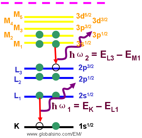
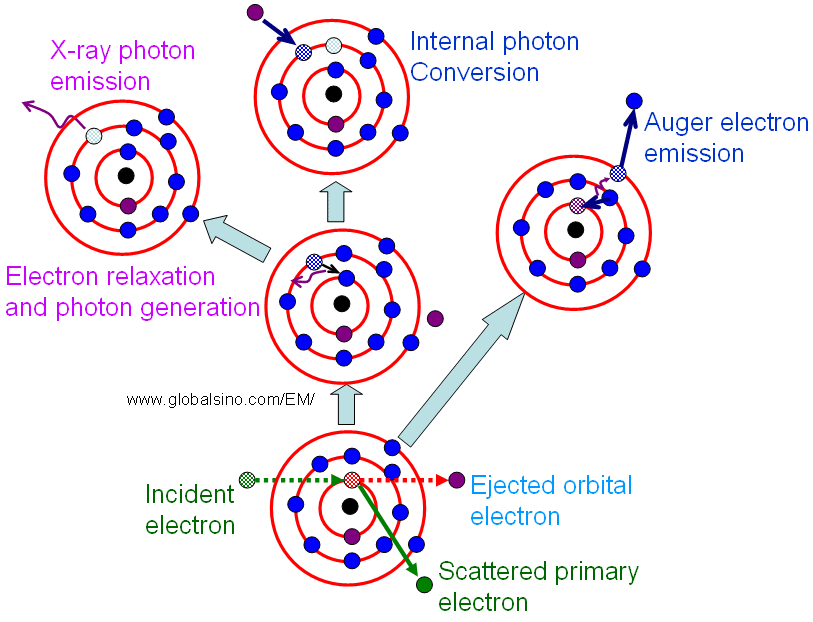
| Before the appearance of EDS (Energy Dispersive Spectrometry) systems, the WDS (wavelength-dispersive spectrometer) had been used for X-ray characterization. EDS was first introduced in the 1960s, when the solid state detectors were first implanted to microanalyzers. EDS is also referred to as Energy Dispersive X-ray (EDX) spectroscopy. An atom is ionized when an inner shell electron is removed by high-energy-electron radiation. To return the excited atom to its ground state, the electron from an outer, higher energy shell fills the vacant inner shell, and then the atom releases an amount of energy equal to the potential energy difference between the two shells. This excess energy, which is unique for every atomic transition, will be emitted by the excited atom either as an X-ray photon (for EDS measurement: Energy Dispersive X-ray Spectrum) or will be self-absorbed and emitted as an Auger electron (for AES measurement: Auger Electron Spectrum). Simply speaking, inelastic scattering mainly involves electron-electron interactions and is mainly applied for analytical analyses such as EELS (electron energy loss spectroscopy) or EDS analysis. Figures 4649a and 4649b shows the principle of X-ray generation in EDS detection. The initial holes can be generated by any energetic beams such as incident electrons in EMs, incident ions in FIB, and laser beams.
Figure 4649a. The principle of X-ray generation.
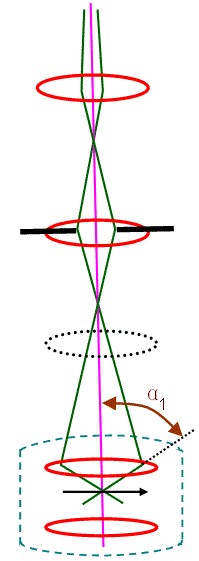
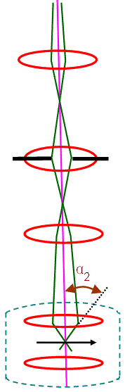
The probe formation in EDS measurement is different from other EM modes. For instance, the schematic illustrations in Figure 4649c show the convergent illumination configurations of various modes in TEMs. In the CTEM condition in Figure 4649c (a), the condenser mini-lens (CM lens) is strongly excited, and incident electrons are focused on the pre-focal point of the objective pre-field, resulting in a parallel illumination on a wide area on the specimen and providing highly coherent electron illumination. In the EDS condition in Figure 4649c (b), the CM lens is turned off and the incident electrons are focused on the specimen by the objective pre-field, resulting in a small-probe illumination. In this case, the illumination angle (α1) is large so that high beam intensity is obtained for a small area in the analytical EDS method. In the NBD mode in Figure 4649c (c), a smaller condenser aperture is used to form a smaller illumination angle (α2). Therefore, a small-diameter probe with relatively high coherence in the illumination is achieved. In the illumination condition in Figure 4649c (c), the illumination angle (α) with a constant probe size can be changed by changing the excitations of the condenser lenses and the CM lens to obtain the incident illumination to form ideal convergent beam electron diffraction (CBED) patterns.
Figure 4649c. Convergent illumination configurations: (a) CTEM mode, (b) EDS mode and (c) NBD mode.
|