Chapter/Index: Introduction | A | B | C | D | E | F | G | H | I | J | K | L | M | N | O | P | Q | R | S | T | U | V | W | X | Y | Z | Appendix
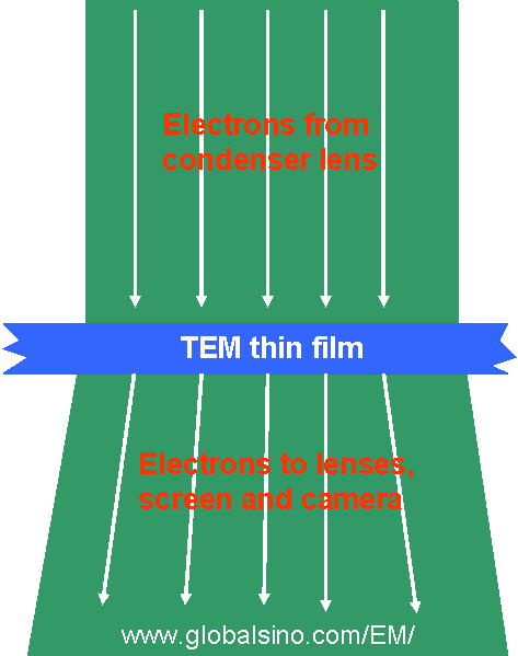
| The comparison of lens conditions between TEM diffraction and TEM imaging modes has been discussed on page2685. One microscope approximately consists of 30 thousands parts. As shown in Figure 4112a, the incident electron beam in CTEM (conventional transmission electron microscopy) is wide and is nearly parallel, irradiating and imaging the whole interest area of the TEM specimen at the common range of 1k × 1k pixels to 10k × 10k pixels. Note that in CTEM the condenser lenses is further used to form a broad parallel beam on the sample. The structure of CTEM systems is described somewhere else.
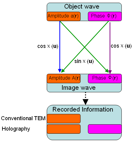
Figure 4112a. The incident electron beam irradiating and imaging An analytical CTEM is able to obtain high resolution transmission electron (HRTEM), bright field (BF) and dark field (DF) images, selected area (SAED) and convergent beam diffraction (CBED) patterns, and characteristic X-ray spectra (EDS) and electron energy loss (EELS) spectra. The wave aberrations (χ) produce a scrambling of amplitude and phase information in the EM (electron microscopy) images. Figure 4112b shows the schematic illustration of the image of a weak object formed by the objective lens. Sin(χ) indicates the cross-talk between amplitude and phase and cos(χ) presents the direct transfer of amplitude or phase information. For instance, in the conventional TEM, the detector only records the image amplitude, while in holography, both the amplitude and phase of the image wave are recorded in the interference fringes of the hologram.
Figure 4112b. Schematic illustration of imaging a weak object. χ represents coherent wave aberration.
Comparing with conventional TEM/STEM, environmental TEM/STEM has advantages as follows:
|