Chapter/Index: Introduction | A | B | C | D | E | F | G | H | I | J | K | L | M | N | O | P | Q | R | S | T | U | V | W | X | Y | Z | Appendix
| Electron holography is a holography with electron waves. ‘Holos’ is a Greek word meaning ‘whole’ and indicating that holograms recorded on photographic films contained all the information required to reconstruct the illuminated object, either in two- (2D) or three-dimensional (3D) formats. Electron holography was initially suggested by Dennis Gabor in 1948 [1, 10] when he was trying to improve the spatial resolution in their electron microscope and to correct its lens aberrations, before the invention of the lasers and its holography application in light optics. The original electron holography work described the reconstruction of an image by illuminating an ‘in-line’ electron hologram with a parallel beam, but the reconstructed image is disturbed by a ‘ghost’ or ‘conjugate’ twin image. The method of electron holography that is most often used for solving problems in materials science is the off-axis, or ‘sideband’, mode. The practical application of electron holography to various materials has been pioneered by some research groups, for instance, by one group at the Hitachi Advanced Research Laboratory in Japan [11]. It is different from conventional HRTEM, in which the phase information and amplitude contrast of the exit electron wave are nonlinearly mixed, electron holography is an interference technique which allows the phase change of the electron waves exiting from the object to be determined and can recover the true object image. Therefore, similar to other methods such as focal series restorations and tilt azimuth restorations, holography has also the advantage of offering both the phase and modulus of the specimen exit plane wave function, free from artifacts, rather than the aberrated image intensity existing in the conventional image. In other words, the electron holography technique overcomes the limitation of most TEM-based methods, i.e. only spatial distributions of image intensity are recorded, and all the information about the phase shift of the incident-electron wave that passes through the specimen is lost. The first attempts to perform the application of electron holography were made on zinc oxide crystals by Haine and Muley at an electron accelerating voltage of 60 keV in 1952 [2], where they obtained crystalline reconstructions at ~ 1 nm resolution. In 1955 G. Möllenstedt and H. Düker [3] invented biprism for electron optics and were for the first time able to record electron holograms in off-axis. Usually, high spatial and temporal coherence of electron beam are required to perform holographic measurements. Therefore, what made electron holography expand into the extremely active field it now is was the appearance of stable coherent field emission guns (FEG) on commercial TEMs (FEGTEMs). In fact, because there were no coherent sources like field emission sources, the realization of Gabor’s holography had been delayed for more than half a century. The high brightness of nanotips allows for short hologram exposure times, therefore, the distortive effects of stray fields on the final image are minimized. A field emission gun (FEG) is needed for electron holography since the spatial coherence with a conventional electron gun extremely limits the resolution. Note that even though for a TEM with a conventional electron gun, a smaller illumination aperture can be used to increase the degree of coherence, the smaller aperture still cannot practically be used for holography measurement because of the smaller coherent beam current Icoh. There are numerous ways of performing electron holography in TEM and STEM. Cowley has highlighted 20 configurations for electron holography [4]. Since the object phase information can be retrieved without transfer gaps, various opportunities appear in both methodical developments and holographic applications in solid state physics, materials science, and chemistry. Nowadays, this technique especially has increasingly been employed as a tool for the measurement of electrostatic and magnetic fields in a variety of samples. Unlike other more direct forms of imaging, holography
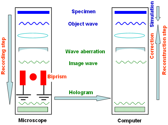
(using electromagnetic, electron, or other kinds of
radiation) is a two-step process (shown in Figure 4309a):
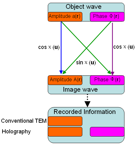
Figure 4309a. Schematic illustration of the two-step holography procedure. In the review paper titled “Tutorial on Off-Axis Electron Holography”, Lehmann and Lichte [12] presented the development of a step-by-step procedure for recording and reconstruction of holograms. The low spherical aberration of the objective lens gives a smaller point resolution as well as produces fewer oscillations of the contrast transfer function (CTF) beyond the point resolution. The accurate determination of the spherical aberration coefficient Cs is very important to many applications of EM techniques, such as electron holography [6, 7], image processing and deconvolution [8], and electron crystallography of proteins [9]. The wave aberrations (χ) produce a scrambling of amplitude and phase information in the EM (electron microscopy) images. Figure 4309b shows the schematic illustration of the image of a weak object formed by the objective lens. Sin(χ) indicates the cross-talk between amplitude and phase and cos(χ) presents the direct transfer of amplitude or phase information. For instance, in the conventional TEM, the detector only records the image amplitude, while in holography, both the amplitude and phase of the image wave are recorded in the interference fringes of the hologram.
Figure 4309b. Schematic illustration of imaging a weak object. χ represents coherent wave aberration.
Table 4309. Characteristics of electron holography technique.
[1] D. Gabor, A new microscopic principle, Nature 4098, 777 (1948).
|