=================================================================================
Different from thermionic emission sources, the field in field emission sources (including cold FEG and thermal FEG) allows the quantum mechanical tunnelling process to occur, where electrons close to the Fermi level are emitted from the tip surface without requiring an input of energy greater than that of the work function. Field-emission
sources consist of pointed tungsten wires (filament emitters) exposed to a high electric field. It is called a “field emission” gun because the electric field causes high-energy electrons to be emitted from a filament emitter. In the case of heated FEGs (Schottky emitters), the tip of the wire is coated with ZrO2 (zirconium oxide) to raise electrical conductivity. Cold FEGs have the main advantage of a small energy spread and a very
long lifetime, but the total current is small and the long-term current stability is
poor.
As shown in Figure 4952, the “extraction” field is generated by the first anode, which is charged by several kV of extraction voltage with respect to the tip. The second anode is then used to accelerate the electrons into the EM (electron microscope) column. The combination of two anodes operates like an electrostatic lens, producing a “virtual” gun crossover. The overall effect of this setup is a dramatic increase in the number of electrons drawn from the tip. The field emission source produces a greater current density than that produced by the thermionic sources and produces ~10 to 100 times higher electron brightness than that of the thermionic single crystal LaB6 emission filament as listed in a table on the comparison of various electron sources in page1409. The main disadvantage for the field emission sources is the requirement of an ultra high column vacuum for the high electric field generated at the tip to maintain a stable emission.
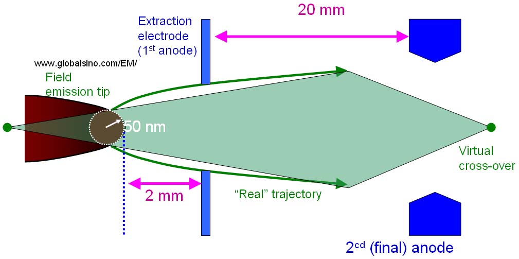
Figure 4952. Schematic illustration of a field-emission source.
The tips have curvatures of 10 to 50 nm in radius.
For a field emission source, the beam of electrons emitted presents an energy profile described by the Fowler-Nordheim (F-N) distribution [1],
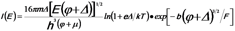 ------------- [4952a] ------------- [4952a]
Δ = µ - E ---------------------- [4952b]
b = 6.8 x 10⁷α
---------------------- [4952c]
where,
µ -- The chemical potential (Typical value ~ 11 eV),
φ -- The work function (for a tungsten tip as 4.5 eV),
α -- The image correction term (Typical value ~ 0.85),
F -- The electric field strength (Typical value ~ 3 x 10⁷ V/m),
E -- The accelerating voltage on the incident electrons.
The F-N energy distribution of emitted electrons includes two distinct regions [2]: a low energy Fermi tail and a high energy tunnelling tail. The low energy Fermi tail is a property of the Fermi surface of the tip material (e.g. tungesten) and is independent of the extraction voltage. The slope of the high energy tunnelling tail is determined by the field strength. Those tails cause beam energy-broadening in field emission guns.
Before the application of field emission electron guns in TEM, the energy resolution of EELS systems had been ~1–2 eV, mainly limited by the energy spreading of thermionic electron source (tungsten filament or LaB6). In the late 1990s, Schottky emission sources became available and have been providing energy resolution greater than 0.5 eV.
In modern STEM systems, a field-emission gun can be used to produce an electron source as small as 3 ~ 10 nm in diameter.
Furthermore, the most promising coherent electron sources for electron microscopes (EMs) have been found in ultrasharp nanotips [3–5] in field emission electron guns due to the very high coherence and significant brightness. The important, common structural feature of their brightest field emitters is that they end with a single atom at the apex of a nanoprotrusion. The resulting characteristics are high coherence, strong focusing, sharp energy spectra, and high degeneracy [6] that significantly improve the spatial and temporal coherence properties. The use of ultrasharp nanotips in the EMs significantly improves the resolution and magnification, and allows for the simultaneous imaging of a larger area.
A field emission gun (FEG) is needed for electron holography since the spatial coherence with a conventional electron gun extremely limits the resolution. Note that even though for a TEM with a conventional electron gun, a smaller illumination aperture can be used to increase the degree of coherence, the smaller aperture still cannot practically be used for holography measurement because of the smaller coherent beam current Icoh.
Both ion getter pumps and cryo-pumps are often employed in applications requiring extremely clean, ultrahigh vacuums, e.g. in LaB6 guns and FEGs.
For TEMs with thermionic electron sources, the MDM (minimum detectable mass) of EDS measurements is in the range of 10-19 to 10-20 g, equivalent to ~100 - ~1000 atoms thick of iron (Fe). For TEMs with FEGs (field emission guns), it is possible to detect a few atoms thick with EDS technique.
[1] Fowler, R.H., Nordheim, L. Electron emission in intense electric fields. Proc. R. Soc. A 119, 173-181 (1928).
[2] Kimoto, K. et al. 0.23eV energy resolution obtained using a cold field-emission gun and a streak imaging technique. Micron 36, 465-469 (2005).
[3] M. Rezeq, J. Pitters, R.A. Wolkow, J. Chem. Phys. 124 (2006)
204716.
[4] V.T. Binh, N. Garcia, Ultramicroscopy 42–44 (1992) 80.
[5] K. Nagaoka, H. Fujii, K. Matsuda, M. Komaki, Y. Murata,
C. Oshima, T. Sakurai, Appl. Surf. Sci. 182 (2001) 12.
[6] V.T. Binh, S.T. Purcell, Appl. Surf. Sci. 111 (1997) 157.
|