
Chapter/Index: Introduction | A | B | C | D | E | F | G | H | I | J | K | L | M | N | O | P | Q | R | S | T | U | V | W | X | Y | Z | Appendix
| The electron beams used in EMs have an energy spread (ΔE) in the range 0.3 to 3 eV, depending on the type of electron source as shown in a table in page1409. For a field emission source, the beam of electrons emitted presents an energy profile described by the Fowler-Nordheim (F-N) Distribution [1], Δ = µ - E ---------------------- [4772b] b = 6.8 x 10⁷α ---------------------- [4772c] where, The F-N energy distribution of emitted electrons includes two distinct regions [2]: a low energy Fermi tail and a high energy tunnelling tail. The low energy Fermi tail is a property of the Fermi surface of the tip material (e.g. tungesten) and is independent of the extraction voltage. The slope of the high energy tunnelling tail is determined by the field strength. Those tails cause beam energy-broadening in field emission guns. The width of the zero-loss peak in EELS spectrum, typically 0.2 – 2 eV, reflects mainly the energy distribution of the electron source. Note that a monochromator for the electron source or data deconvolution is necessary in the frontiers of TEM-EELS if the energy spread of the available electron source in TEM is larger than the intrinsic fine structures of spectra. In STEM, the fluctuations in accelerating voltage or the current flow in the probe-forming electromagnetic lenses contributes to the chromatic aberration that leads a cutoff to the highest spatial frequency. In HRTEM, the cut-off frequency corresponds to the information limit. In STEM, the effect of the fluctuations induces additional contribution to the probe size [3], where, In summary, the energy spread of the electron beam is mainly induced by: Due to the significant energy spread in the electron beam, the chromatic aberration associated with the lenses will lead to image degradation in TEM as listed in Table 4772. On the other hand, according to Equation 4772d, i) and ii) above induces also an increase in probe size in the scanning modes (e.g. SEM and STEM). This effect of the energy spread (ΔE) is proportional to ΔE/E0. Table 4772. Causes of energy spreads and the image degradation induced by the associated lenses.
Furthermore, for TEM analysis, the size of electron source must be large to achieve a large area of illumination with sufficient electron density. From this point of view, thermionic sources are more than capable of meeting these criteria. However, this relatively large source size in addition to a large electron energy spread means that thermionic sources are not applicable to scanning probe microscopy and EELS microanalysis.
[1] Fowler, R.H., Nordheim, L. Electron emission in intense electric fields. Proc. R. Soc. A 119, 173-181 (1928).
|
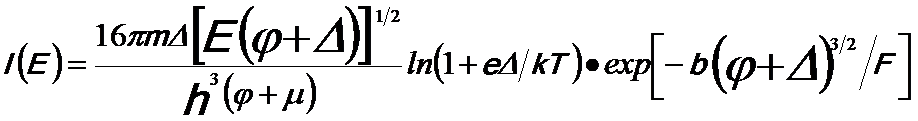 ------------- [4772a]
 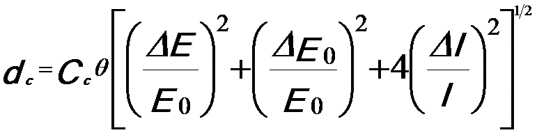 ------------- [4772d]