Chapter/Index: Introduction | A | B | C | D | E | F | G | H | I | J | K | L | M | N | O | P | Q | R | S | T | U | V | W | X | Y | Z | Appendix
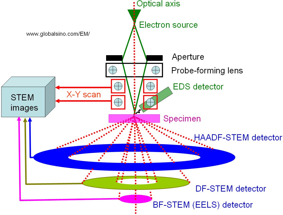
| In general, a low voltage STEM is a hybrid instrument with the features of SEM and TEM with a convergent probe, while a high voltage TEM is a hybrid instrument with the features of TEM with both a parallel beam (for TEM function) and a convergent probe (for STEM function). STEM was invented by von Ardenne, German in 1937. [1] However, the application of STEM was not successful until several decades later, first performed by Albert Crewe in 1970.[2] Figure 4538a shows the positions of the detectors which can be installed in a STEM system. Depending on the scattering angle of the transmitted electrons, various signals can be detected as a function of the position of the scanning probe: BF (bright-field)-STEM, DF (dark-field)-STEM or HAADF (high angle annular dark field)-STEM. The DF detectors are annularly shaped to maximize the collection efficiency and the range of the collected scattering angles can be adjusted through the magnification of the intermediate lenses.
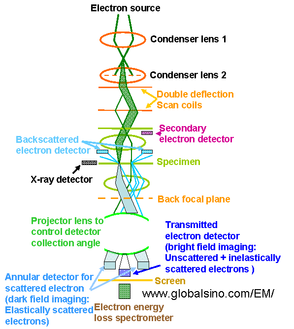
Figure 4538a. The positions of detectors in STEMs. The schematics in Figure 4538b shows the electron optical column in a modern analytical electron microscope operated in STEM mode.
Figure 4538b. Schematics of the electron optical column in a modern
[1] Von Ardenne M, Beischer DZ. Electrochemie 1940;46:270–7.
|