Chapter/Index: Introduction | A | B | C | D | E | F | G | H | I | J | K | L | M | N | O | P | Q | R | S | T | U | V | W | X | Y | Z | Appendix
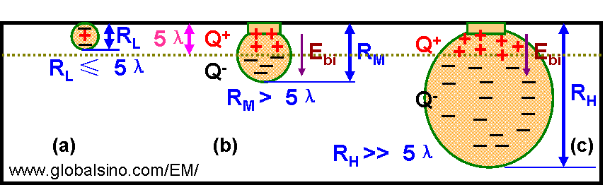
| A change in accelerating voltage changes the secondary electron to backscattered electron ratio, resulting in contrast changes. The emission of secondary electrons (SEs) from a given spot size or probe current will remain relatively constant as the accelerating voltage changes. However as the accelerating voltage is increased, the electron beam penetration and diffusion become larger and results in signal (electrons coming out of the sample surface) being generated from deeper within the specimen as well as the backscattered electron (BSE) influence increases, diminishing the contribution to the image from secondary electrons. This can obscure fine surface structures. Furthermore, increased BSE enhances the contrast based on composition. The solution for obtaining fine surface structure is generally to use lower kVs such as 5 - 10 kV. Based on the dependence of interaction volume and maximum escape depth on PE (primary electron) beam energy, there are three different cases regarding SE emissions: i) RL ≤ 5λ, ii) RM > 5λ, and iii) RH >> 5λ as shown in Figure 4858a (R is maximum interaction volume and λ is maximum escape depth). For the case of R ≤ 5λ, the two positive and negative charge areas are very close. For the cases of R > 5λ and R >> 5λ, there are two distinct regions inside the interaction volume: a thin near-surface layer with thickness T ~ 5λ in positive charge Q+, and a negatively charged bulk (Q-) with a thickness of about (R–T). As a result, the implanted charge is ΔQ = Q+ + Q-, and the built-in electric field (Ebi) governed by ΔQ is established.
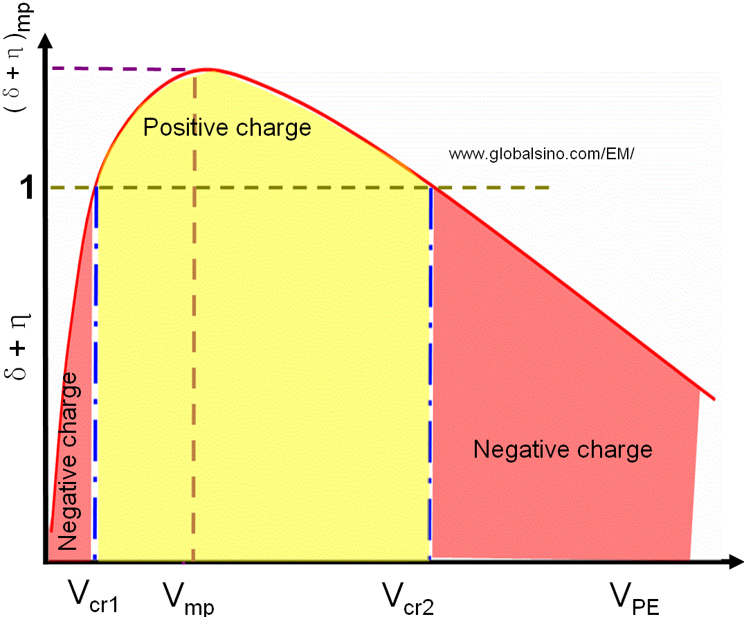
Figure 4858b shows the schematic illustration of the SE yield d as a function of the accelerating voltage of primary electrons (VPE). δmp represents the maximum yield at the most probable energy (MPE) of SE emission (Vmp). Vcr1 and Vcr2 are two critical voltages at which δ is equal to 1. Typically, Vcr1 is < 100 V and Vcr2 about 2 kV for insulators [1].
Figure 4858b. Schematic illustration of the SE yield d as a function of the For biological materials, due to the relatively low acceleration voltage of the cryo-SEM (e.g. 30 kV) in comparison with a cryo-TEM (normally 80–300 kV), the SEM contrast between the vitreous ice and the cells is still very strong even though without chemical staining.
[1] Reimer, L. (1993) Specimen charging and damage. Image Formation in Low Voltage Scanning Electron Microscopy, Chap. 5, pp. 71 - 135. SPIE Press, Bellingham.
|