|
CMOS 工艺流程
P-well process:
Similar to n-well process except a p-well is implanted rather than an n-well.

Produces n- and p-transistors that are more balanced.
Transistors that reside in the native substrate tend to have better characteristics.
In general, p-devices are lower gain than n-devices.
Therefore, p-well process naturally moderate the differences.
CMOS Processing Technology
Twin-tub process:
Allows independent optimization of gain, threshold voltage, etc. of n-type and p-type devices.

Both types of substrate contacts are REQUIRED in this process.
CMOS Processing Technology
Silicon-On-Insulator (SOI) process:
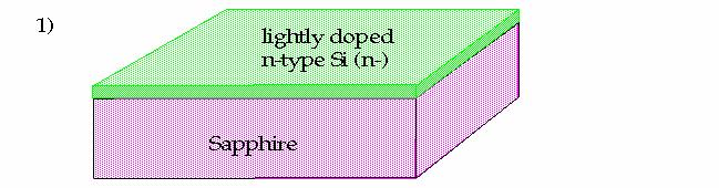
Instead of silicon substrate, use an insulating substrate.
Silicon can be grown on:
Sapphire or
SiO2 which in turn has been grown on silicon.
CMOS Processing Technology

Advantages:
Closer packing of p- and n-transistors, due to absence of wells.
Absence of latch-up problems (to be discussed).
Only "sidewall" areas of source and drain diffusions contribute to parasitic junction capacitance, faster devices.
Leakage currents to substrate and adjacent devices almost eliminated.
Enhanced radiation tolerance.
Disadvantages:
No substrate diodes, inputs more difficult to protect.
Device gains are lower, I/O structures must be larger.
Density of contemporary digital processes is actually determined by number and density of metal interconnection layers.
Sapphire and silicon on SiO 2 substrates are considerably more expensive.
CMOS Processing Technology
CMOS Enhancements:
More levels of metal interconnect, 2, 3, 4, ...
Eases automated routing and improves power and clock distribution to modules.
"Vias" are used to connect upper layers of metal to metal 1.
"Contact cuts" are made from metal 1 to diffusion or poly.
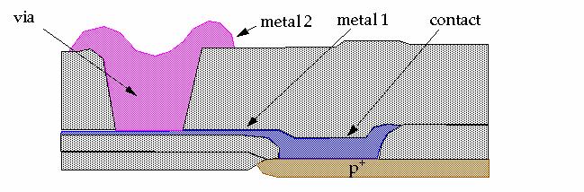
Aggressive processes allow the stacking of vias on top of contacts.
[1]|[2]
其他推荐阅读:
|
